Elastic packaging structure for semiconductor chip

A packaging structure and semiconductor technology, applied in the direction of semiconductor devices, semiconductor/solid-state device components, electric solid-state devices, etc., can solve the problems of high packaging cost, short service life, poor environmental adaptability, etc., to improve yield and reduce packaging The effect of high cost and high voltage level

Pending Publication Date: 2019-10-25
GLOBAL ENERGY INTERCONNECTION RES INST CO LTD
View PDF0 Cites 2 Cited by
  • Summary
  • Abstract
  • Description
  • Claims
  • Application Information

AI Technical Summary

Problems solved by technology

[0004] In order to overcome the disadvantages of high packaging cost, poor environmental adaptability and short service life in the above-mentioned prior art, the present invention provides an elastic packaging structure for semiconductor chips, including an upper electrode, a lower electrode, a ring-shaped packaging structure and a plurality of chip sub-structures. unit; a plurality of chip sub-units are arranged between the upper electrode and the lower electrode; the annular packaging structure is sealed and arranged on the side of the upper electrode and the lower electrode and forms a closed shell structure with the upper electrode and the lower electrode, which can effectively reduce the packaging cost, improve the environmental adaptability of semiconductor chips, and prolong the service life of semiconductor chips

Method used


Image

  • Elastic packaging structure for semiconductor chip
  • Elastic packaging structure for semiconductor chip

Examples


Embodiment Construction

[0047] The present invention will be described in further detail below in conjunction with the accompanying drawings.

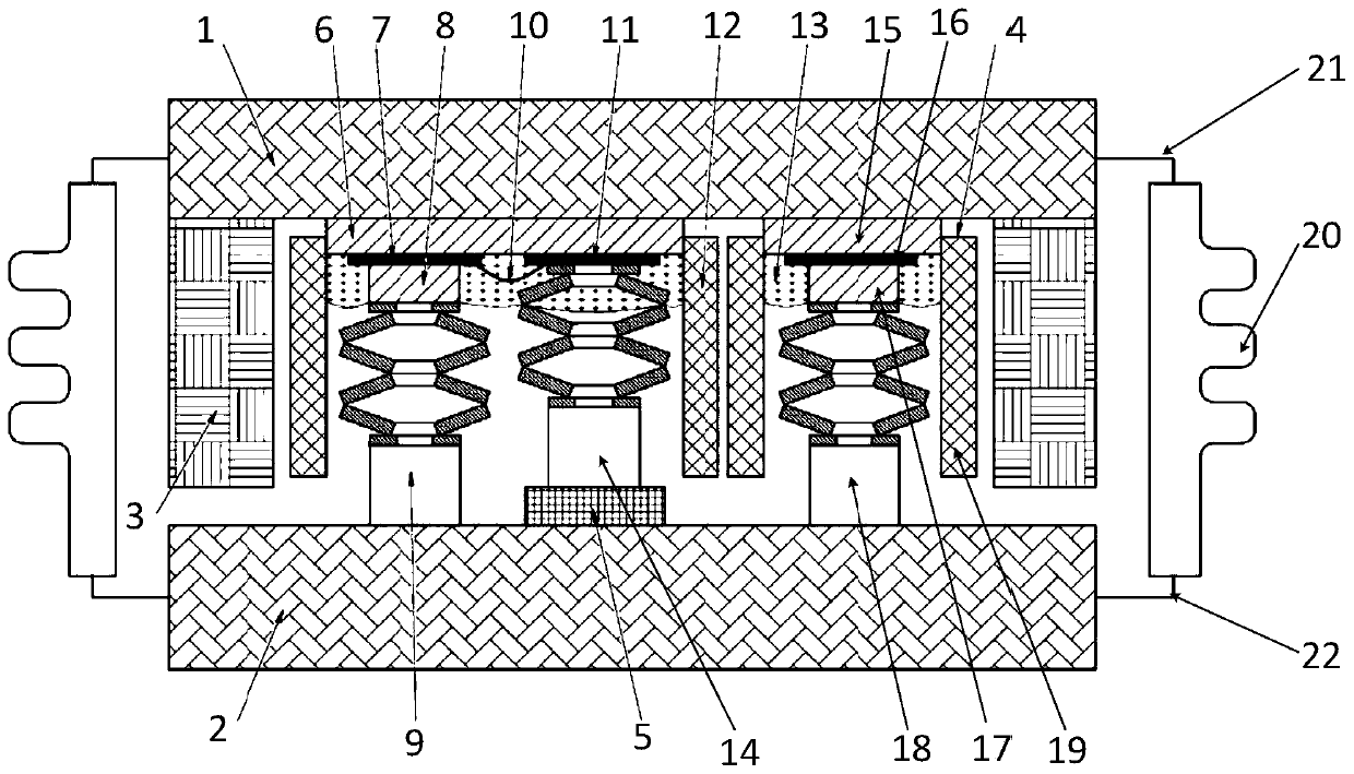
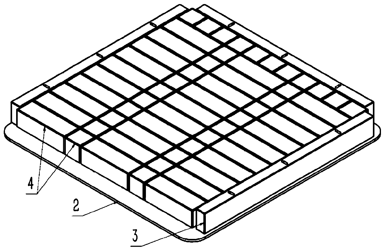
[0048] An embodiment of the present invention provides an elastic packaging structure for a semiconductor chip, such asfigure 1 As shown, it includes an upper electrode 1, a lower electrode 2, an annular packaging structure 20 and a plurality of chip subunits 4;

[0049] A plurality of chip sub-units 4 are arranged between the upper electrode 1 and the lower electrode 2; the annular packaging structure 20 is sealed and arranged on the sides of the upper electrode 1 and the lower electrode 2 and forms a closed shell structure with the upper electrode 1 and the lower electrode 2.

[0050] The elastic packaging structure provided by the embodiment of the present invention also includes an upper flange 21 and a lower flange 22;

[0051] The upper electrode 1 is welded to the annular packaging structure 20 through the upper flange 21 , and the lower electrode 2 is...


PUM


Abstract

The invention provides an elastic packaging structure for a semiconductor chip. The elastic packaging structure comprises an upper electrode, a lower electrode, an annular packaging structure and a plurality of chip subunits, wherein the plurality of chip subunits are arranged between the upper electrode and the lower electrode; the annular packaging structure is arranged on the side edges of theupper electrode and the lower electrode in a sealed mode and forms a closed tube shell structure with the upper electrode and the lower electrode. According to the invention, the packaging cost can beeffectively reduced, the environmental adaptability of the semiconductor chip is improved, the service life of the semiconductor chip is prolonged, the universality is high, the packaging cost of semiconductor chip failure can be reduced to the greatest extent, and the packaging yield of the semiconductor chip is remarkably improved. The tube shell structure is a sealed structure, so the adaptability of the semiconductor chip to the application environment can be greatly improved; the tube shell structure is filled with the silica gel, so the insulation and voltage resistance of the semiconductor chip can be greatly improved, the voltage class of the semiconductor chip is higher, and the reliability of the semiconductor chip is higher.

Description

technical field [0001] The invention relates to the technical field of power semiconductors, in particular to an elastic packaging structure for semiconductor chips. Background technique [0002] The packaging structure of semiconductor chips is divided into rigid packaging and elastic packaging according to the pressure contact method. Among them, in the rigid package, both sides of the chip are in contact with metal hard surfaces. This type of structure is simple, but it has high requirements for chip thickness consistency and pressure uniformity. It also has high requirements for the surface processing accuracy of internal structural parts and heat sinks used in applications. strict. As the device capacity increases and the number of internal chips increases, the pressure and crimping area will increase accordingly, making it more difficult to realize large-area high-precision processing. Due to the hard contact between the chip and the metal structure, the pressure dif...

Claims


Application Information

Patent Timeline
Patent Type & Authority Applications(China)
IPC IPC(8): H01L23/31H01L25/065
CPCH01L23/31H01L25/065
Inventor 吴军民林仲康张朋陈中圆王耀华武伟唐新灵孙帅张西子张雷李现兵王亮张喆韩荣刚石浩
Owner GLOBAL ENERGY INTERCONNECTION RES INST CO LTD
Why Eureka
Try Eureka