A kind of atomic layer deposition equipment and gas transmission method

A technology of atomic layer deposition and gas transmission, applied in coating, gaseous chemical plating, metal material coating process, etc., can solve problems such as vacuum pump stuck, improve reliability and life, and reduce the risk of stuck Effect

Active Publication Date: 2021-10-15
BEIJING NAURA MICROELECTRONICS EQUIP CO LTD
View PDF7 Cites 0 Cited by
  • Summary
  • Abstract
  • Description
  • Claims
  • Application Information

AI Technical Summary

Problems solved by technology

[0008] The purpose of the present invention is to provide an atomic layer deposition equipment and gas transmission method to solve the problem in the prior art that various precursor precursors react in the vacuum pump to form powder, causing the vacuum pump to be stuck

Method used


Image

  • A kind of atomic layer deposition equipment and gas transmission method
  • A kind of atomic layer deposition equipment and gas transmission method
  • A kind of atomic layer deposition equipment and gas transmission method

Examples


Embodiment Construction

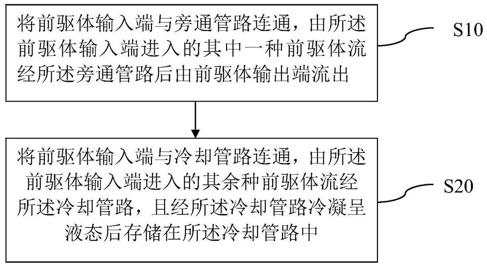
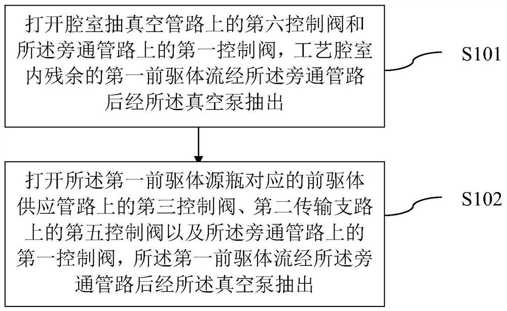
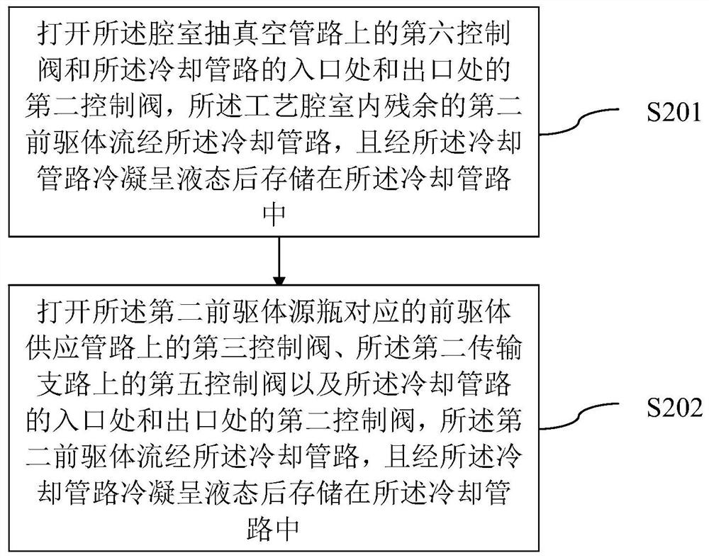
[0049] The present invention proposes a method for realizing a novel atomic layer deposition process, which sets a cooling pipeline to condense precursors flowing through the pipeline and stores them in the pipeline to prevent multiple precursors from entering the vacuum pump at the same time.

[0050] The present invention will be described in more detail below with reference to the accompanying drawings. Although preferred embodiments of the invention are shown in the drawings, it should be understood that the invention may be embodied in various forms and should not be limited to the embodiments set forth herein. Rather, these embodiments are provided so that this disclosure will be thorough and complete, and will fully convey the scope of the disclosure to those skilled in the art.

[0051] image 3 An atomic layer deposition apparatus according to an exemplary embodiment of the present invention is shown. Such as image 3 As shown, the atomic layer deposition equipment...


PUM


Abstract

The invention discloses an atomic layer deposition equipment and a gas transmission method. The device includes a bypass pipeline and a cooling pipeline, the cooling pipeline is used to condense and store at least one precursor, wherein the bypass pipeline and the cooling pipeline are connected in parallel to the input end of the precursor and the precursor output terminal, and the precursor input terminal is selectively communicated with the bypass pipeline or the cooling pipeline. In the present invention, cooling pipelines are set to condense the precursors flowing through the pipelines, and store them in this section of pipelines to prevent multiple precursors from entering the vacuum pump at the same time, thereby reducing the number of precursors produced by the reaction of multiple precursors in the vacuum pump. powder, which reduces the risk of the vacuum pump being stuck due to powder accumulation, thereby improving the reliability and life of the vacuum pump operation.

Description

technical field [0001] The invention relates to the field of semiconductor integrated circuit manufacturing, in particular to an atomic layer deposition device and a gas transmission method. Background technique [0002] Atomic layer deposition (ALD) technology is a method that can coat substances layer by layer on the surface of a substrate in the form of a single atomic film. In the process of atomic layer deposition, the chemical reaction of a new layer of atomic film is directly related to the previous layer. In this way, only one layer of atoms is deposited in each reaction, that is, monoatomic layer deposition, also known as atomic layer epitaxy ( atomic layer epitaxy). At first, due to the low deposition rate of this process, its application was limited, but with the development of microelectronics and deep submicron chip technology, the size of devices and materials is continuously reduced, and the aspect ratio of devices is increasing. Atomic layer deposition techn...

Claims


Application Information

Patent Timeline
Patent Type & Authority Patents(China)
IPC IPC(8): C23C16/455C23C16/52
CPCC23C16/45527C23C16/45544C23C16/52
Inventor 徐宝岗
Owner BEIJING NAURA MICROELECTRONICS EQUIP CO LTD
Why Eureka
Try Eureka