Thin Film Chip-on-Chip Packaging Structure
A technology of film-on-chip packaging and pins, which is applied in semiconductor/solid-state device components, semiconductor devices, electrical components, etc., can solve the problems of difficult increase in the number of bumps and limited number of pins, etc., and reduce local sinking or bending , improve the quality, the effect of stress distribution average
- Summary
- Abstract
- Description
- Claims
- Application Information
AI Technical Summary
Problems solved by technology
Method used
Image

Examples
Embodiment Construction
[0048] Reference will now be made in detail to the exemplary embodiments of the present invention, examples of which are illustrated in the accompanying drawings. Wherever possible, the same reference numbers will be used in the drawings and description to refer to the same or like parts.
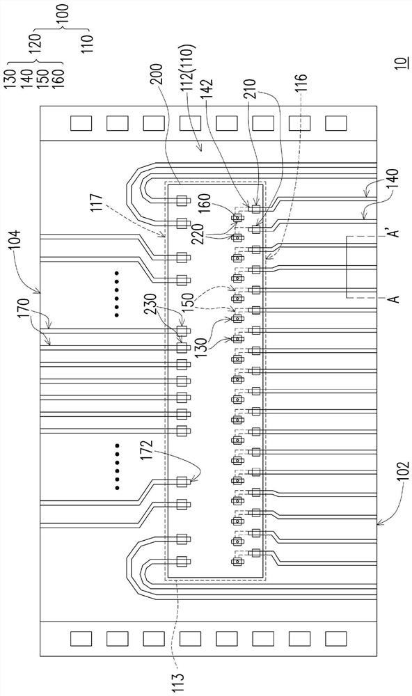
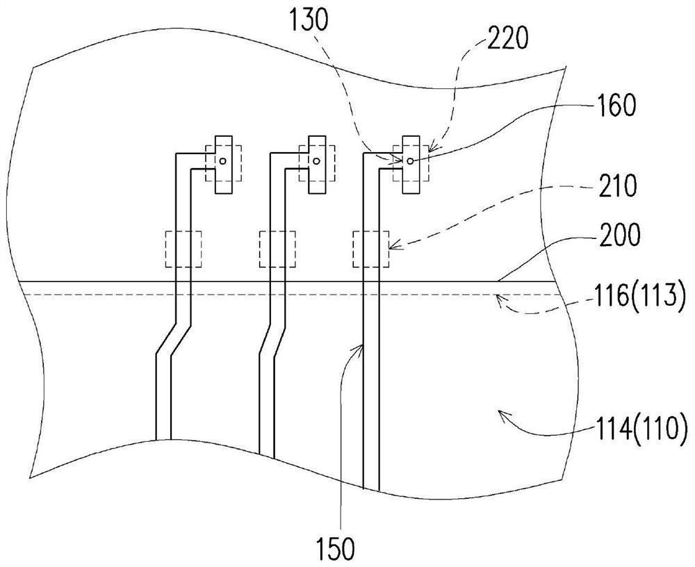
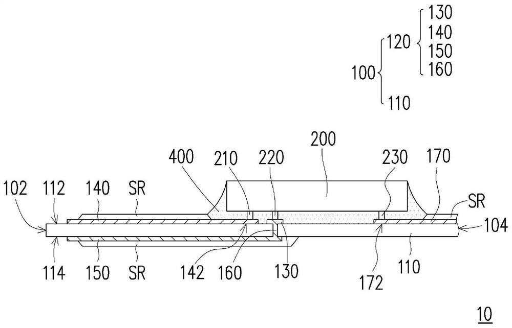
[0049] figure 1 A schematic top view of a chip-on-film packaging structure according to an embodiment of the present invention is shown. figure 2 shown as figure 1 A partially enlarged schematic bottom view of the thin film chip-on-chip packaging structure shown. image 3 shown as figure 1 A schematic partial cross-sectional side view of the thin film chip-on-chip packaging structure. Please refer to figure 1 , figure 2 and image 3 , the film-on-chip packaging structure 10 of this embodiment includes a flexible circuit carrier 100 and a chip 200 . The flexible circuit carrier 100 includes a flexible substrate 110 and a circuit structure 120 . The flexible substrate 110 includes ...
PUM
 Abstract
Description
Claims
Application Information