Flexible array substrate and flexible display panel
A flexible array and substrate technology, which is applied in the direction of electrical components, electric solid devices, circuits, etc., can solve problems such as metal wiring breakage and large stress of metal wiring on flexible array substrates, so as to improve reliability and avoid metal wiring breakage Effect
- Summary
- Abstract
- Description
- Claims
- Application Information
AI Technical Summary
Problems solved by technology
Method used
Image

Examples
Embodiment 1
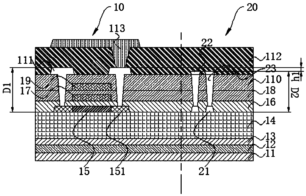
[0027] Such as figure 1 Shown is a schematic structural diagram of Embodiment 1 of the flexible array substrate of the present invention. Wherein, the flexible array substrate includes a display area 10 and a bending area 20 located on one side of the display area 10, and the flexible array substrate also includes a first flexible substrate 11, a water-oxygen barrier layer 12, a second flexible substrate Bottom 13, buffer layer 14 and array structure layer;
[0028] The part of the array structure layer located in the display area 10 has a first source-drain wiring 111, the part of the array structure layer located in the bending area 20 has a second source-drain wiring, and the second The relative distance between the source-drain wiring and the buffer layer 14 is smaller than the relative distance between the first source-drain wiring 111 and the buffer layer 14 .
[0029] Specifically, the array structure layer also includes an active layer 15, a first gate insulating lay...
Embodiment 2
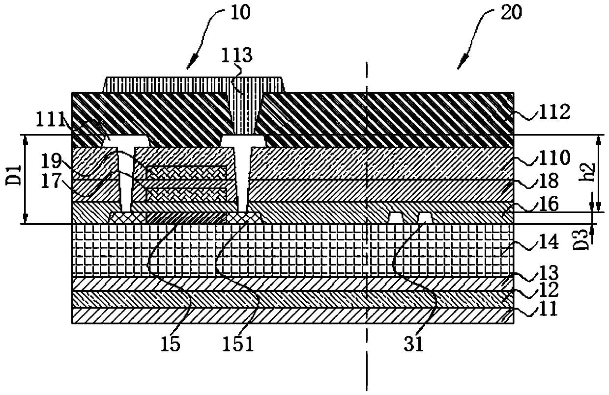
[0047] A flexible array substrate, such as image 3 As shown, the only difference from Embodiment 1 is that the second source-drain wiring 31 is located on the buffer layer 14 , the first gate insulating layer 16 and the second gate insulating layer 18 on any of the layers. The relative distance D3 between the second source-drain wiring 31 and the buffer layer 14 is smaller than the relative distance D1 between the first source-drain wiring 111 and the buffer layer 14 . Therefore, there is a certain height difference h2 between the source and drain traces of the flexible substrate located in the bending region 20 and the source and drain traces of the flexible substrate located in the display region 10 . The difference h2 can couple the stress between the flexible array substrate and the source-drain wiring, so that in the process of bending the flexible array substrate, the source-drain wiring located in the bending region of the flexible array substrate The stress received...
Embodiment 3
[0049] A flexible array substrate, such as Figure 4 As shown, the only difference from Embodiment 1 is that the second source-drain wiring 41 is located on the interlayer insulating layer 110 . The relative distance D4 between the second source-drain wiring 41 and the buffer layer 14 is smaller than the relative distance D1 between the first source-drain wiring 111 and the buffer layer 14 . Therefore, there is a certain height difference h3 between the source and drain traces of the flexible substrate located in the bending region 20 and the source and drain traces of the flexible substrate located in the display region 10 . The difference h3 can couple the stress between the flexible array substrate and the source-drain wiring, so that in the process of bending the flexible array substrate, the source-drain wiring located in the bending region of the flexible array substrate The stress received is small, the source and drain wires are prevented from being broken during the ...
PUM
 Abstract
Description
Claims
Application Information
 - R&D
- Intellectual Property
- Life Sciences
- Materials
- Tech Scout
- Unparalleled Data Quality
- Higher Quality Content
- 60% Fewer Hallucinations
Browse by: Latest US Patents, China's latest patents, Technical Efficacy Thesaurus, Application Domain, Technology Topic, Popular Technical Reports.
© 2025 PatSnap. All rights reserved.Legal|Privacy policy|Modern Slavery Act Transparency Statement|Sitemap|About US| Contact US: help@patsnap.com