Display substrate and preparation method and repair method thereof, and display device
A technology for a display substrate and a repair method, which is applied in the directions of organic semiconductor devices, electrical components, and electric solid-state devices, and can solve the problems of pixel driving circuit damage and low success rate.
- Summary
- Abstract
- Description
- Claims
- Application Information
AI Technical Summary
Problems solved by technology
Method used
Image

Examples
no. 1 example
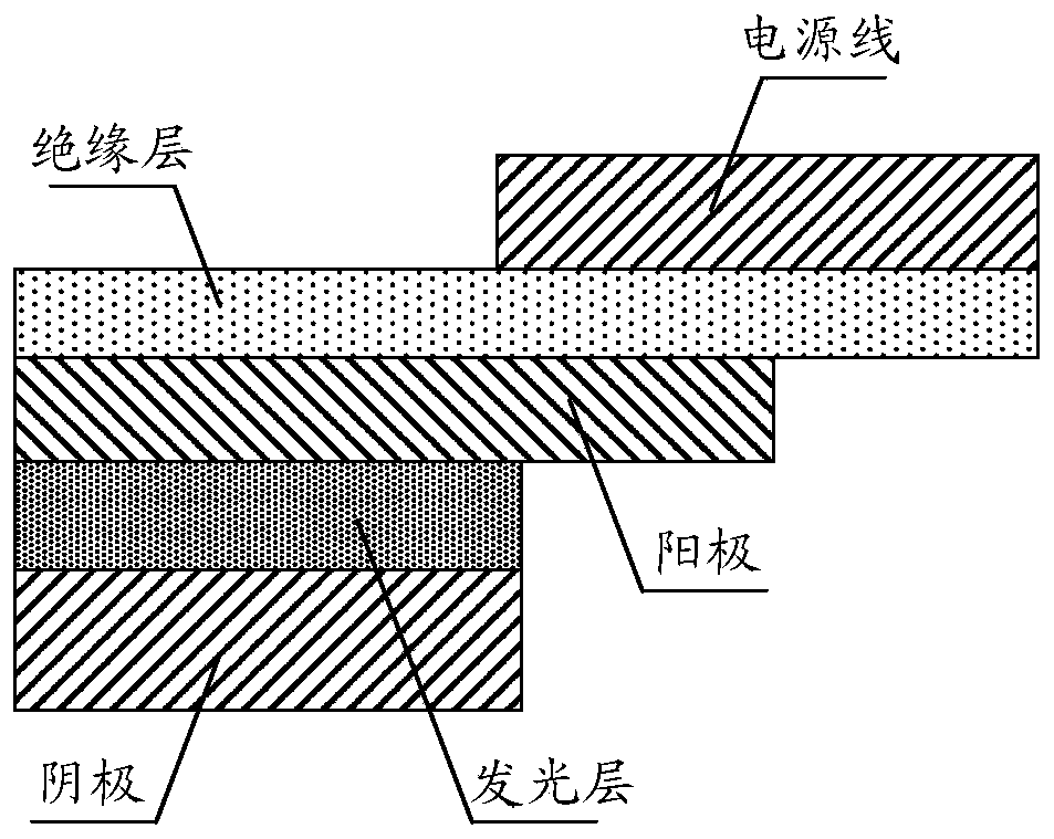
[0078] Figure 7 A schematic structural diagram of the first embodiment of the substrate is shown for the present invention. Such as Figure 7 shown and combined with Figure 8 ~ Figure 21 , this embodiment shows that the substrate includes:
[0079] base 10;
[0080] The gate line GN, the first gate electrode 11, the second gate electrode 21, the first capacitor electrode 31 and the repair electrode 40 arranged on the substrate 10;
[0081] The first insulating layer 12 covering the gate line GN, the first gate electrode 11, the second gate electrode 21, the first capacitor electrode 31 and the repair electrode 40;
[0082] The first active layer 13, the second active layer 23 and the second capacitive electrode 32 arranged on the first insulating layer 12;
[0083] Covering the first active layer 13, the second active layer 23 and the second insulating layer 14 of the second capacitive electrode 32, a plurality of via holes are opened on the second insulating layer 14, an...
no. 2 example
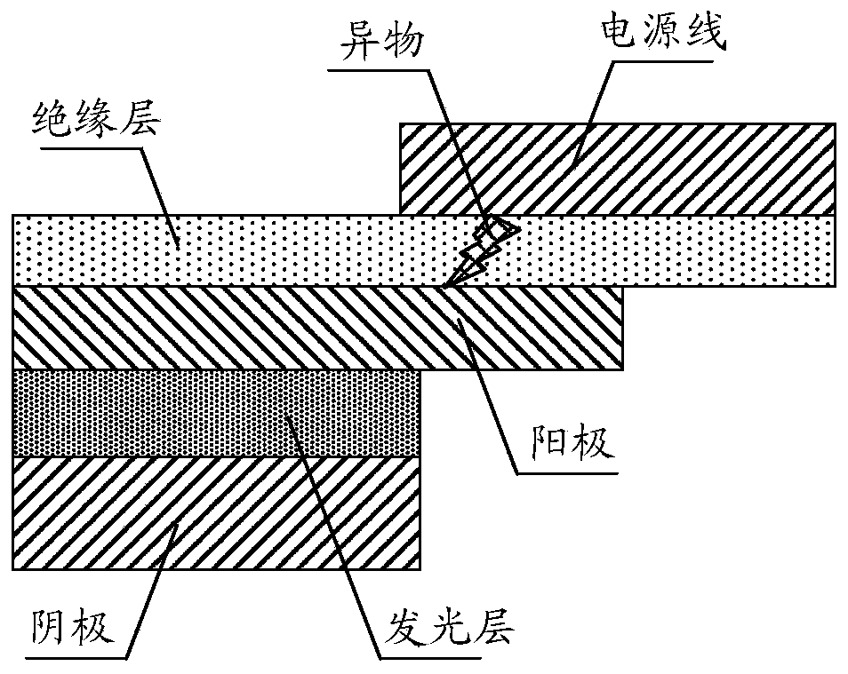
[0107] Figure 22 A schematic structural diagram of the second embodiment of the substrate is shown for the present invention. This embodiment is an extension of the aforementioned first embodiment. This embodiment shows that the main structure of the substrate is basically the same as that of the aforementioned first embodiment. The repair electrode 40 and the gate line are arranged on the same layer. The lines FV are arranged on the same layer, the first insulating layer 12 and the second insulating layer 14 are separated between the repair electrode 40 and the first drain electrode 16 and the auxiliary cathode line FV, and the repair electrode 40 and the auxiliary cathode line FV have a second overlapping area. Such as Figure 22 As shown, the difference is that in the substrate structure shown in this embodiment, the first drain electrode 16 is connected to the repair electrode 40 through the tenth via hole.
[0108] Figure 23 It is a schematic diagram of repairing def...
no. 3 example
[0112] Figure 24 A schematic structural diagram of a third embodiment of the substrate is shown for the present invention. This embodiment is an extension of the aforementioned first embodiment. This embodiment shows that the main structure of the substrate is basically the same as that of the aforementioned first embodiment. The repair electrode 40 and the gate line are arranged on the same layer. The lines FV are arranged on the same layer, the first insulating layer 12 and the second insulating layer 14 are separated between the repair electrode 40 and the first drain electrode 16 and the auxiliary cathode line FV, and the repair electrode 40 and the auxiliary cathode line FV have a second overlapping area. Such as Figure 24 As shown, the difference is that in the substrate structure shown in this embodiment, the auxiliary cathode line FV is connected to the repair electrode 40 through the eleventh via hole.
[0113] Figure 25 It is a schematic diagram of repairing de...
PUM
| Property | Measurement | Unit |
|---|---|---|
| Power | aaaaa | aaaaa |
Abstract
Description
Claims
Application Information
 - R&D
- Intellectual Property
- Life Sciences
- Materials
- Tech Scout
- Unparalleled Data Quality
- Higher Quality Content
- 60% Fewer Hallucinations
Browse by: Latest US Patents, China's latest patents, Technical Efficacy Thesaurus, Application Domain, Technology Topic, Popular Technical Reports.
© 2025 PatSnap. All rights reserved.Legal|Privacy policy|Modern Slavery Act Transparency Statement|Sitemap|About US| Contact US: help@patsnap.com