Method and system for recording working state of digital logic design engineering

A design engineering and digital logic technology, which is applied in the field of recording the working status of digital logic design engineering, can solve problems such as user difficulties, limited signal length, and FPGA debugging work difficulties, and achieve the effect of improving work efficiency and lasting for a long time

Pending Publication Date: 2019-11-19
INSPUR ARTIFICIAL INTELLIGENCE RES INST CO LTD SHANDONG CHINA
View PDF3 Cites 0 Cited by
  • Summary
  • Abstract
  • Description
  • Claims
  • Application Information

AI Technical Summary

Problems solved by technology

The current FPGA debugging mainly uses the online debugging tools provided by the manufacturer. The signal recording function of the tools requires FPGA on-chip resources as storage, and the length of the stored signals is limited. Observing the changes between signals brings great difficulties to FPGA debugging

Method used


Image

  • Method and system for recording working state of digital logic design engineering

Examples


Embodiment Construction

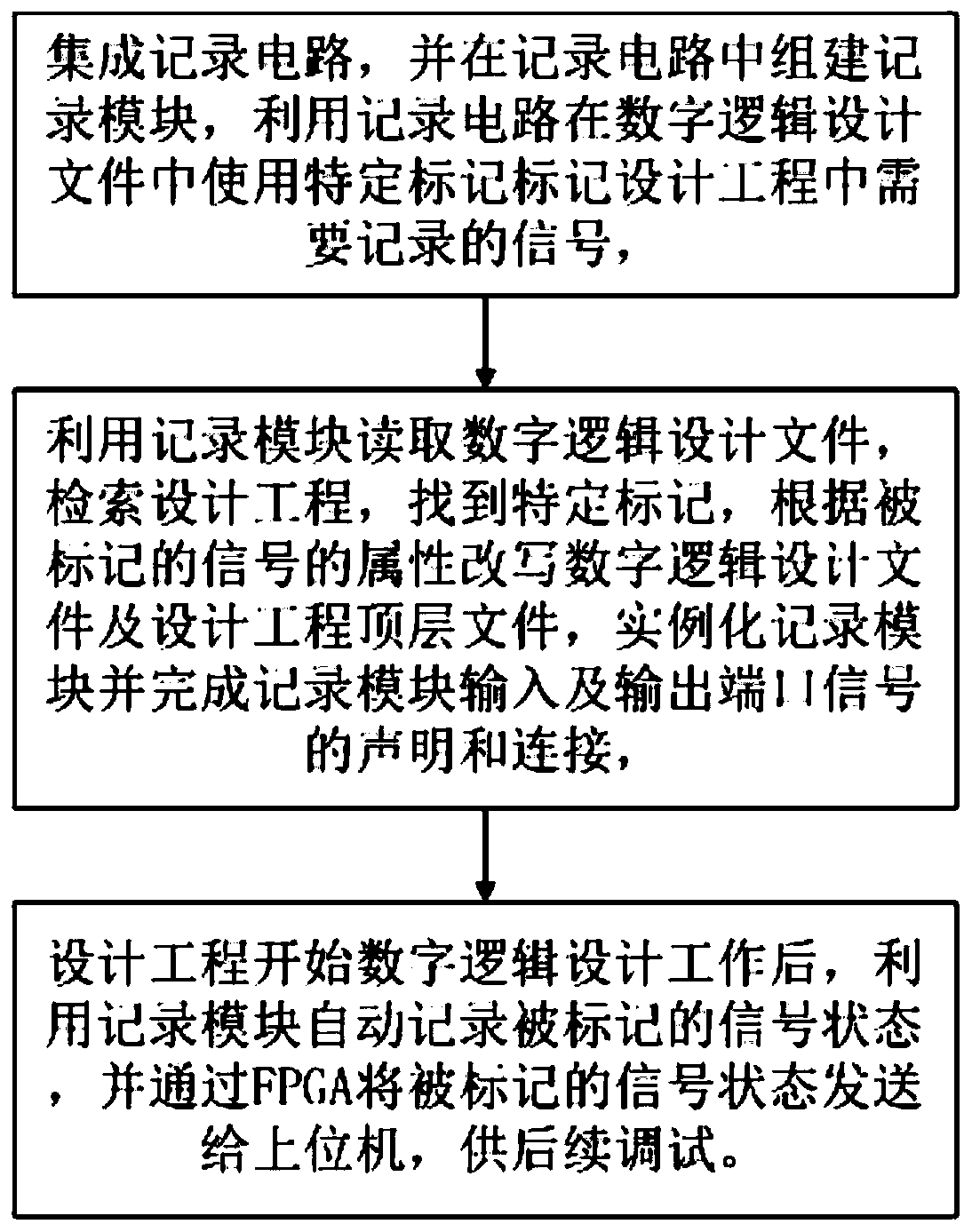
[0025] The invention provides a system for recording the working state of digital logic design engineering, which includes a recording circuit, and a recording module is built in the recording circuit, and the recording circuit uses specific marks in the digital logic design file to mark the signals that need to be recorded in the design project.

[0026] The recording module reads the digital logic design file, retrieves the design project, finds a specific mark, rewrites the digital logic design file and the top-level file of the design project according to the attributes of the marked signal, instantiates the recording module and completes the declaration of the input and output port signals of the recording module and connect,

[0027] After the design project starts the digital logic design work, the recording module automatically records the marked signal state, and sends the marked signal state to the host computer through the FPGA for subsequent debugging.

[0028] At ...


PUM


Abstract

The invention discloses a method and system for recording the working state of a digital logic design project, and relates to the technical field of digital logic design. Signals needing to be recorded in a design project are marked by using specific marks in a digital logic design file by utilizing a recording circuit; a recording module is used for reading the digital logic design file, retrieving design engineering, finding specific markers, rewriting a digital logic design file and a design engineering top layer file according to the attribute of the marked signal; the recording module isinstantiated, declaration and connection of input and output port signals of the recording module are completed, after digital logic design work of a design project is started, the recording module isused for automatically recording the marked signal state, and the marked signal state is sent to the upper computer through the FPGA for subsequent debugging.

Description

technical field [0001] The invention discloses a method and system for recording the working state of a digital logic design project, and relates to the technical field of digital logic design. Background technique [0002] With the continuous development of silicon technology, the scale of digital logic design is getting larger and larger, and it is becoming more and more difficult to verify the function of the design, and it is difficult to guarantee the completeness of the design. Before ASIC tape-out of the design, performing functional simulation on the FPGA board is an effective measure that can greatly reduce the risk of tape-out failure. Currently FPGA debugging mainly uses the online debugging tools provided by the manufacturer. The signal recording function of the tools requires FPGA on-chip resources as storage, and the length of the stored signals is limited. Observing the changes between signals has brought great difficulties to FPGA debugging. [0003] The pr...

Claims


Application Information

Patent Timeline
IPC IPC(8): G06F11/22G06F11/26
CPCG06F11/2268G06F11/2273G06F11/26
Inventor 赵鑫鑫李朋秦刚姜凯
Owner INSPUR ARTIFICIAL INTELLIGENCE RES INST CO LTD SHANDONG CHINA
Why Eureka
Try Eureka