

A tp scanning method applied to idc chips
A scanning method and chip technology, applied in the field of TP scanning, can solve problems such as large system noise and achieve the effect of improving SNR
- Summary
- Abstract
- Description
- Claims
- Application Information
AI Technical Summary
Problems solved by technology
Method used
Image

Examples
Embodiment Construction
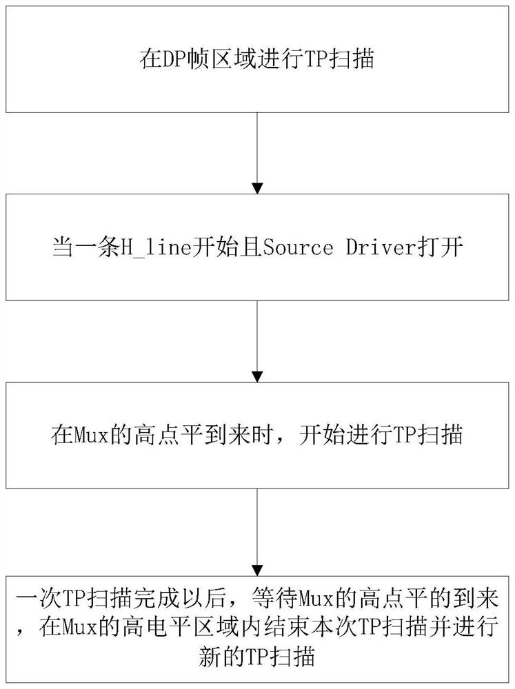
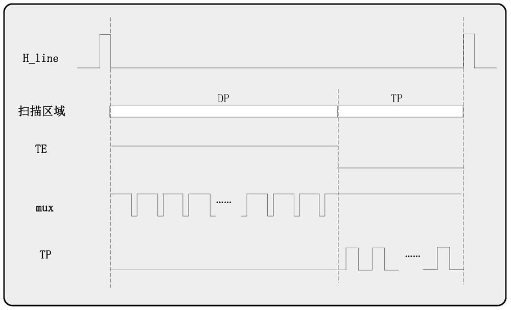
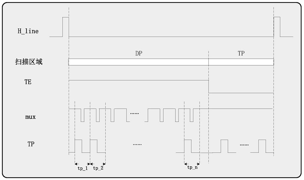
[0015] In the IDC chip, the n-way Mux signals in DP are integrated into one signal, and sent to TP through DP, and DP will also send one signal TE to TP. When TE is high, it means that DP is in the display state; TE is low. When the level is high, it means that the display of DP on one H_line has been completed.
[0016] Traditional scanning modes such as figure 2 As shown, when TE is pulled high, TP scanning is not performed because it is in the DP frame area. When the falling edge of TE is collected, it means that the display of DP has been completed, and Mux will not switch again. At this time, the noise is relatively small, and the scanning time of TP starts. Before the arrival of the next H_line, TP completes scanning in the TP frame area, and transmits the analog signal collected by CA to ADC, ADC completes decoding and transmits the digital signal to CPU for calculation and processing. Depend on figure 2 It can be seen that the scanning time in the TP frame area is...
PUM
 Abstract
Description
Claims
Application Information