Display substrate, manufacturing method thereof and display device

A technology for display substrates and substrate substrates, which is used in the manufacture of semiconductor/solid-state devices, electrical components, and electrical solid-state devices.

Inactive Publication Date: 2019-11-22
BOE TECH GRP CO LTD +1
View PDF3 Cites 11 Cited by
  • Summary
  • Abstract
  • Description
  • Claims
  • Application Information

AI Technical Summary

Problems solved by technology

[0004] However, the storage capacitor occupies a certain area in the pixel unit, and the storage capacitor cannot transmit light, so the area of ​​the light-transmitting region of the pixel unit is small, and the aperture ratio of the display substrate is low.

Method used


Image

  • Display substrate, manufacturing method thereof and display device
  • Display substrate, manufacturing method thereof and display device
  • Display substrate, manufacturing method thereof and display device

Examples


Embodiment Construction

[0095] In order to make the purpose, technical solution and advantages of the application clearer, the application will be further described in detail below in conjunction with the accompanying drawings. Apparently, the described embodiments are only some of the embodiments of the application, not all of them. Based on the embodiments in this application, all other embodiments obtained by persons of ordinary skill in the art without making creative efforts belong to the scope of protection of this application.

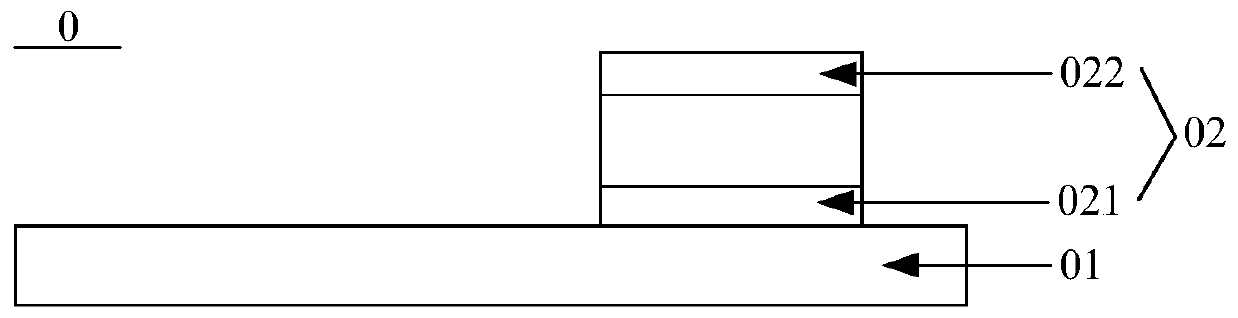
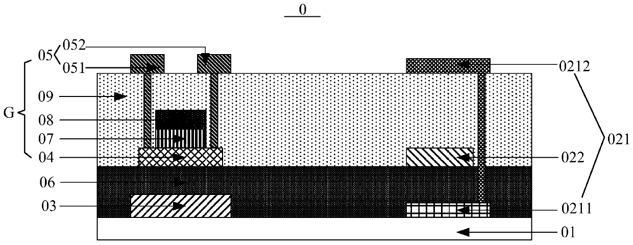
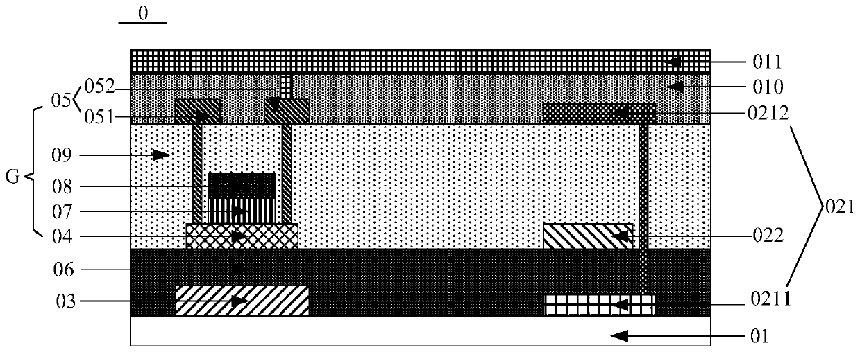
[0096] Please refer to figure 1 , which shows a schematic structural diagram of a display substrate 0 provided by an embodiment of the present application, see figure 1 , the display substrate 0 includes a base substrate 01, and the pixel unit ( figure 1 not shown in ), the pixel unit includes a storage capacitor 02, and the plate of the storage capacitor 02 is a transparent plate.

[0097] To sum up, in the display substrate provided by the embodiment of the present...


PUM


Abstract

The invention discloses a display substrate, a manufacturing method thereof and a display device, and belongs to the technical field of display. The display substrate comprises a substrate body and apixel unit located on the substrate body, wherein the pixel unit comprises a storage capacitor, and a polar plate of the storage capacitor is a transparent polar plate. Because the polar plate of thestorage capacitor is a transparent polar plate, the storage capacitor can transmit light, and the light transmission area of the pixel unit is large. The aperture opening ratio of the display substrate can be improved. The manufacturing method is used for manufacturing the display substrate.

Description

technical field [0001] The present application relates to the field of display technology, in particular to a display substrate, a manufacturing method thereof, and a display device. Background technique [0002] With the continuous development of the display industry, users have higher and higher requirements for display substrates, and high-quality display substrates are more favored by users. [0003] At present, the display substrate includes a plurality of pixel units defined by intersections of data lines and gate lines, and each pixel unit includes a pixel electrode, a thin film transistor (English: Thin Film Transistor; TFT for short) and a storage capacitor electrically connected to the pixel electrode. , the TFT is used to apply an electrical signal to the pixel electrode during the scanning phase, and the storage capacitor is used to maintain the potential of the pixel electrode during the non-scanning phase. Wherein, the pole plate of the storage capacitor is us...

Claims


Application Information

Patent Timeline
Patent Type & Authority Applications(China)
IPC IPC(8): H01L27/12H01L21/77H01L49/02
CPCH01L27/1255H01L27/1259H01L28/60H01L27/1225H01L29/78633H01L27/1248H01L27/127
Inventor 王东方苏同上
Owner BOE TECH GRP CO LTD
Why Eureka
Try Eureka