

Automatic injection molding system for semiconductor component packaging and working method of automatic injection molding system
A technology of injection molding system and working method, applied in coating and other directions, which can solve the problems of poor quality consistency and labor-intensive
- Summary
- Abstract
- Description
- Claims
- Application Information
AI Technical Summary
Problems solved by technology
Method used
Image

Examples
Embodiment Construction
[0025] The technical solution of the present invention will be described in further non-limiting detail below in combination with preferred embodiments and accompanying drawings.
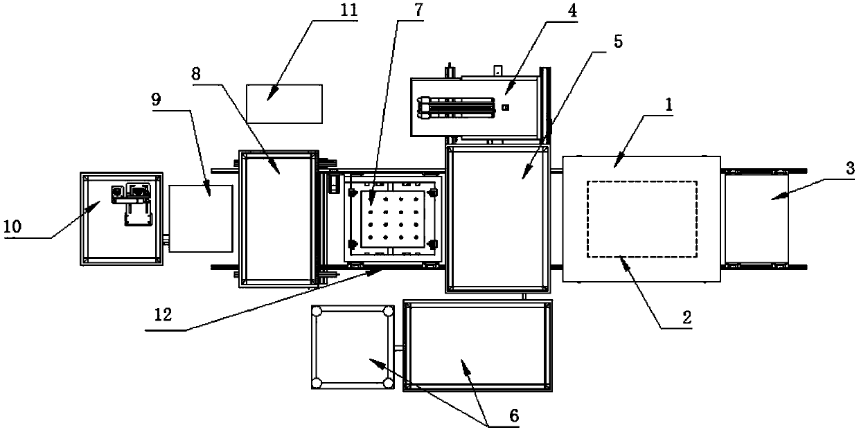
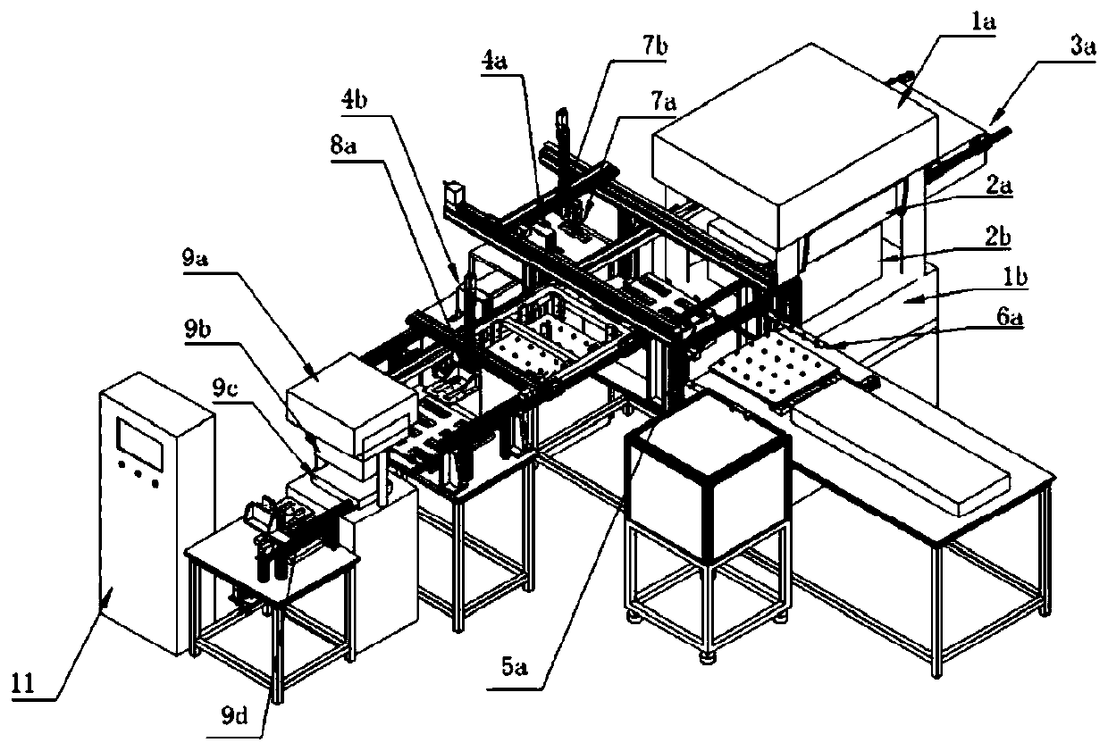
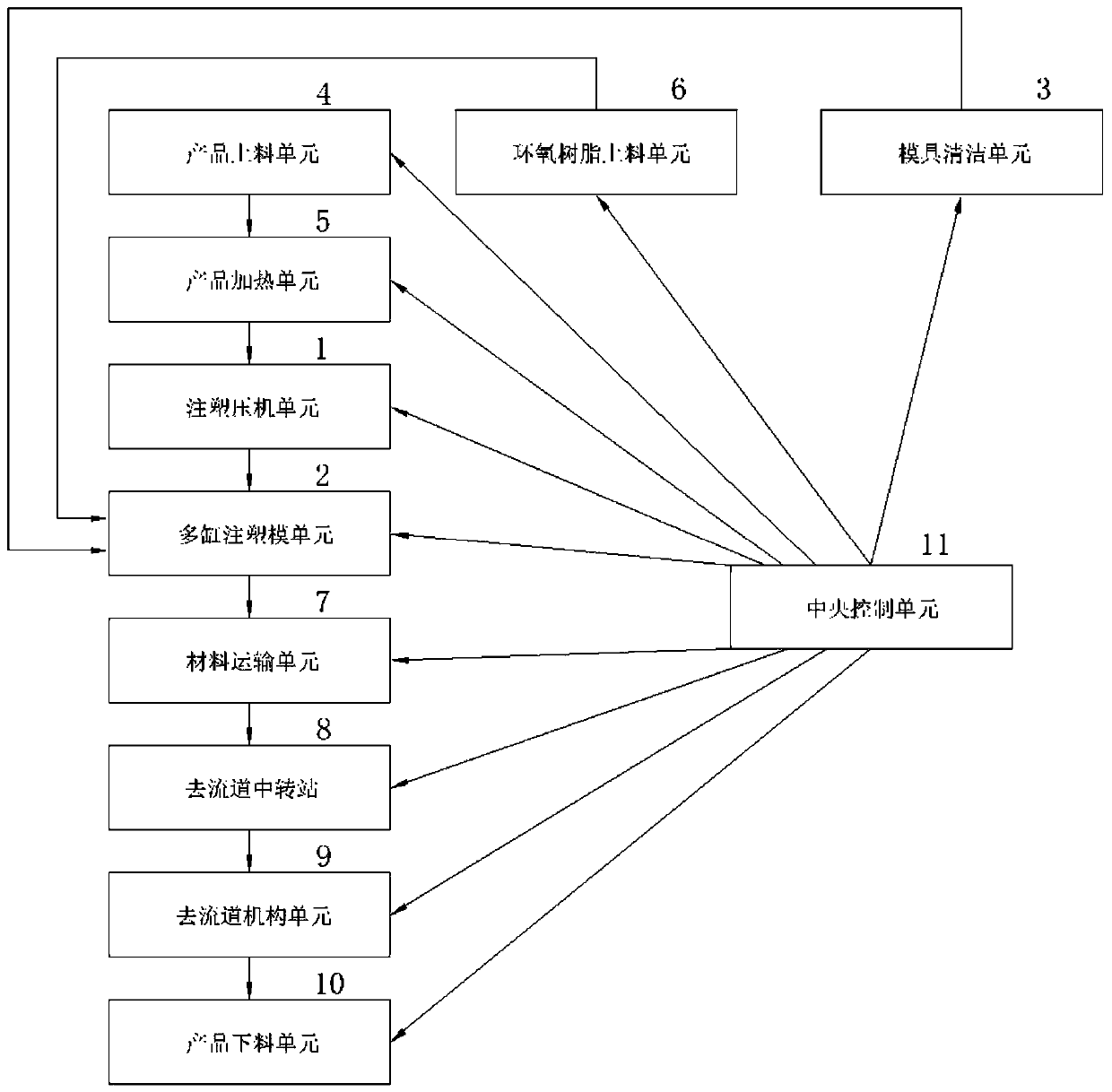
[0026] Such as figure 1 , figure 2 The semiconductor component packaging automatic injection molding system shown includes injection molding press unit 1, multi-cylinder injection mold unit 2, mold cleaning unit 3, product feeding unit 4, product heating unit 5, epoxy resin feeding unit 6, material The transportation unit 7, the transfer station 8 to the runner, the mechanism unit 9 to the runner, the product unloading unit 10, the central control unit 11 and the rack platform 12 required by each system.
[0027] The product loading unit 4 includes a material box transportation input device, a material box lifting control device 4a, a product pushing mechanism and a material box transportation output device 4b. Carry the material box full of products to the corresponding position of the product e...
PUM
 Abstract
Description
Claims
Application Information