

Sputtering target for transparent conductive film
A technology of transparent conductive film and sputtering target, which is applied in the direction of sputtering coating, conductive layer on insulating carrier, circuit, etc., can solve the problems of high resistance, poor productivity, low etching processability of conductive film, etc., and achieve high Resistivity, less nodules and arcing, and high film resistivity effects
- Summary
- Abstract
- Description
- Claims
- Application Information
AI Technical Summary
Problems solved by technology
Method used
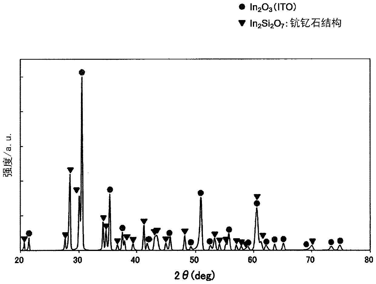
Image

Examples
Embodiment
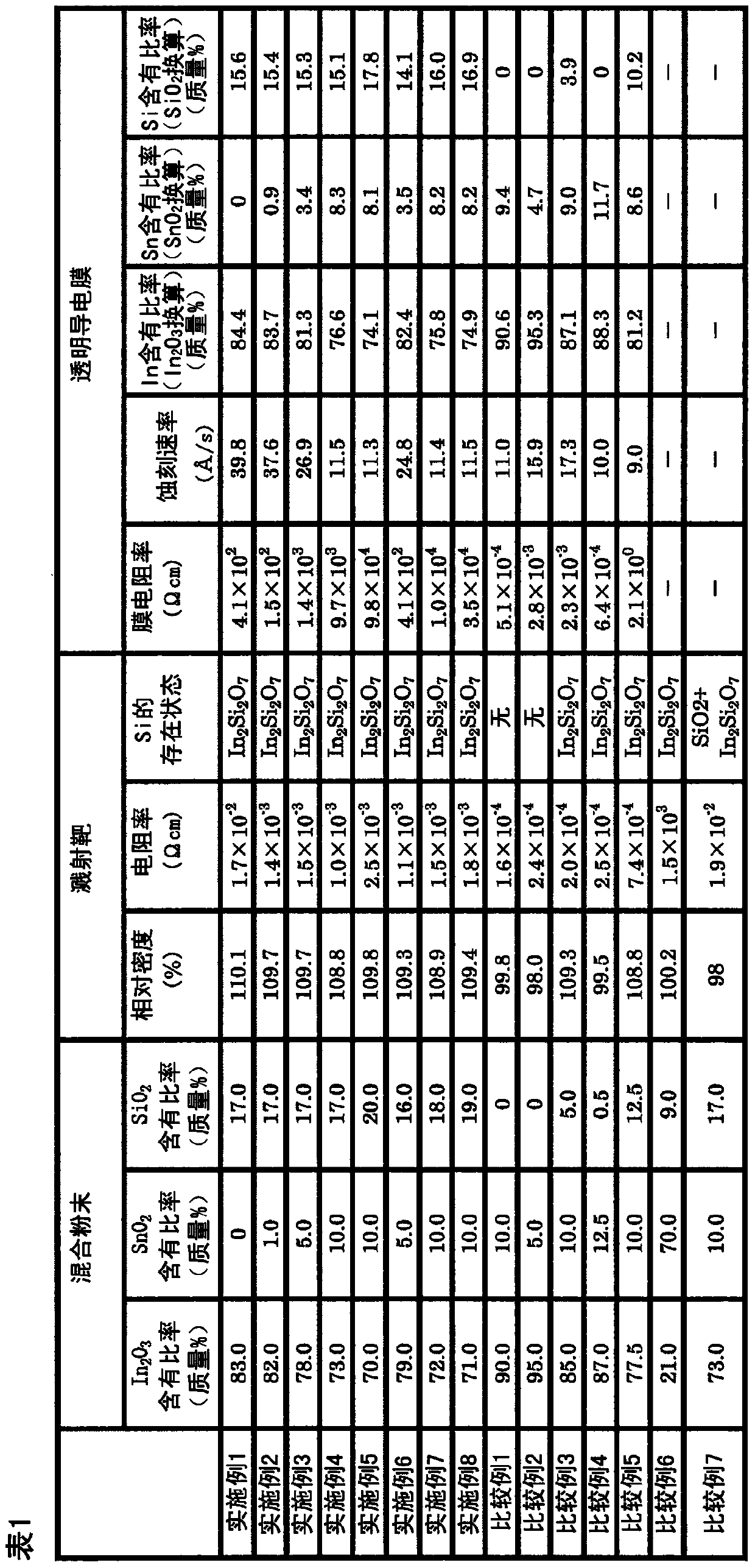
[0055] The measurement methods used in the following Examples and Comparative Examples are shown below.
[0056] 1. The relative density of the target
[0057] The relative density of the sputtering target for transparent conductive films was measured based on the Archimedes method. Specifically, by dividing the mass of the target in the air by the volume (the mass of the target in water / the specific gravity of water at the measurement temperature), the theoretical density ρ (g / cm 3 ) as the relative density (unit: %).
[0058] ρ=((C1 / 100) / ρ1+(C2 / 100) / ρ2+…+(Ci / 100) / ρi) -1 (X)
[0059] (In the formula, C1~Ci represent the contents (mass%) of the constituent substances of the target, respectively, and ρ1~ρi represent the densities (g / cm3) of each constituent substance corresponding to C1~Ci 3 ). )
[0060] In the following examples and comparative examples, the substance (raw material) used for the manufacture of the target is In 2 o 3 , SnO 2 , SiO 2 , therefore, for ...
PUM
| Property | Measurement | Unit |
|---|---|---|
| density | aaaaa | aaaaa |
Abstract
Description
Claims
Application Information