

Inverted light-emitting element
A light-emitting element and flip-chip technology, applied in the direction of electrical components, semiconductor devices, circuits, etc., can solve problems such as chip leakage failure, epitaxial layer peeling off, chip aging failure, etc., and achieve the effect of improving reliability and reducing interface voids
- Summary
- Abstract
- Description
- Claims
- Application Information
AI Technical Summary
Problems solved by technology
Method used
Image

Examples
Embodiment 1
[0022] The structure of the present invention is illustrated below in conjunction with the manufacturing method,
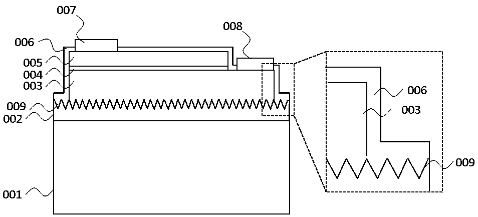
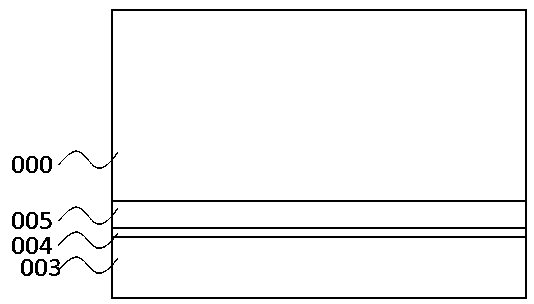
[0023] (1) if figure 2 As shown, an epitaxial structure of a flip-chip light-emitting element is provided, which includes: an epitaxial growth substrate 000, a p-type conductive layer 003, a quantum well 004, and an n-type conductive layer 005;
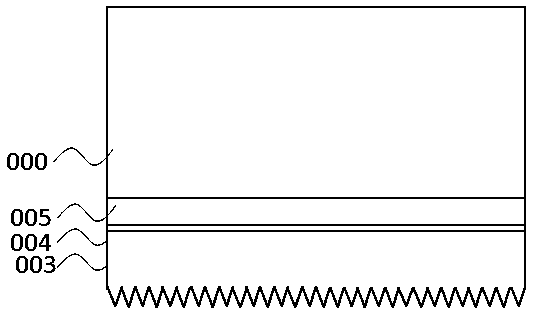
[0024] (2) if image 3 As shown, through the roughening process, a roughened surface is formed on the surface of the p-type conductive layer 003, and the roughness of the surface is 300 nanometers;
[0025] (3) if Figure 4 As shown, a transparent bonding layer 002 is deposited on the surface of the roughened p-type conductive layer 003, and the surface of the transparent bonding layer 002 is polished;
[0026] (4) if Figure 5 As shown, the epitaxial layer (including p-type conductive layer 003, quantum well 004, and n-type conductive layer 005) is bonded to the transparent substrate 001 through the transparent bond...
PUM
 Abstract
Description
Claims
Application Information