Multichannel voltage difference sampling circuit and method

A voltage difference, sampling circuit technology, applied in the direction of measuring current/voltage, measuring electrical variables, measuring devices, etc., can solve the problems of large power consumption loop stability, cumbersome circuits, etc., to achieve strong adaptability, circuit power consumption, etc. Drop, the effect of simple circuit structure

Active Publication Date: 2019-12-17
SOUTH CHINA UNIV OF TECH
View PDF9 Cites 2 Cited by
  • Summary
  • Abstract
  • Description
  • Claims
  • Application Information

AI Technical Summary

Problems solved by technology

For this kind of circuit, the subtraction circuit built by op amp is more commonly used. This kind of circuit consumes a lot of power and needs to pay attention to the stability of the loop.
As an energy storage element, capacitors are often used in sampling schemes, and are mostly used in sample and hold circuits, but the circuits in the solution of differential (differential) voltage sampling are relatively cumbersome

Method used


Image

  • Multichannel voltage difference sampling circuit and method
  • Multichannel voltage difference sampling circuit and method
  • Multichannel voltage difference sampling circuit and method

Examples


Embodiment 1

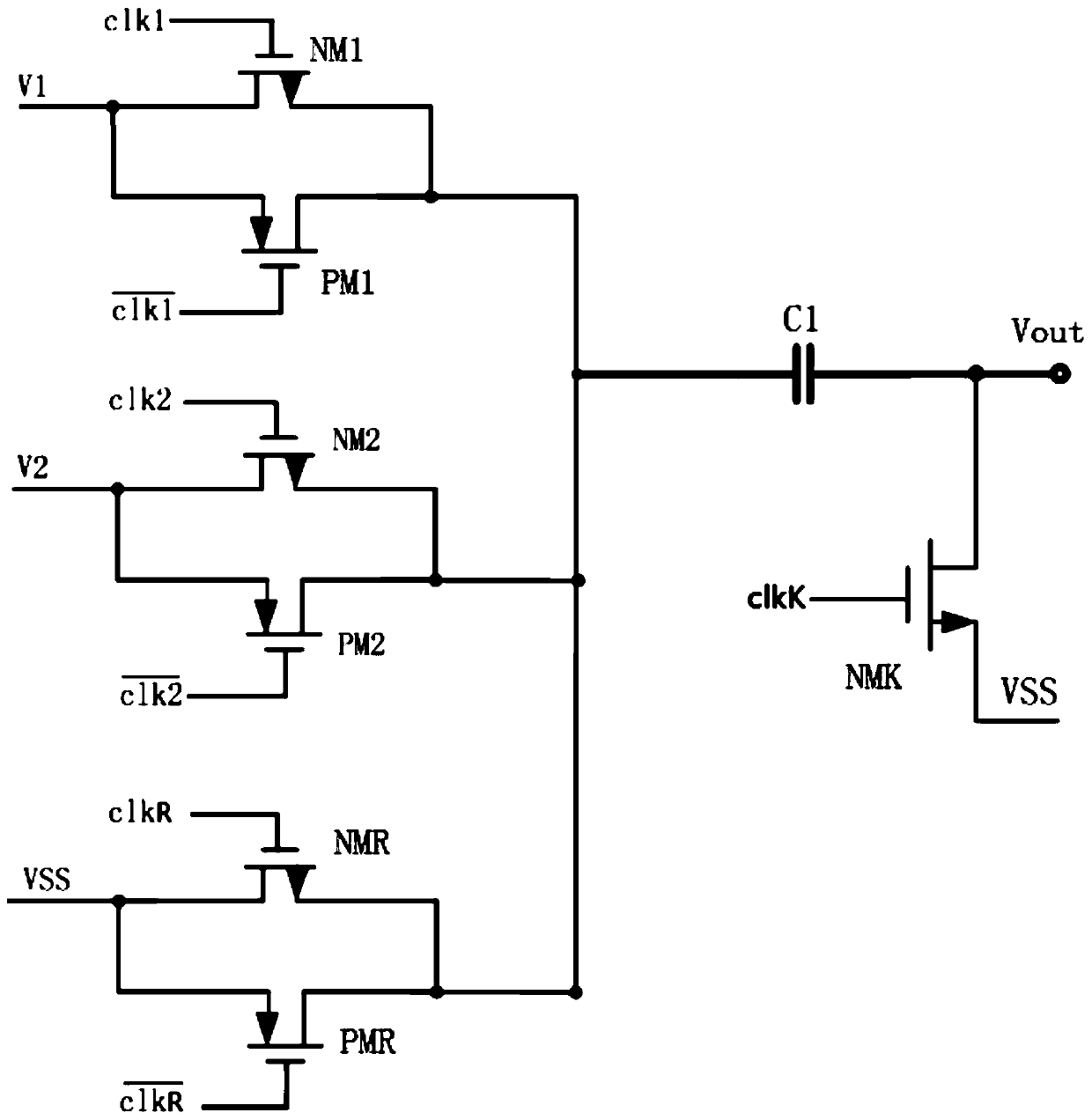
[0018] This embodiment is the simplest mode, there are only two voltage inputs to be sampled, such as figure 1 shown. The first NMOS transistor NM1 and the first PMOS transistor PM1, the second NMOS transistor NM2 and the second PMOS transistor PM2 are paired to form a gate unit, and the reset NMOS transistor and the reset PMOS transistor are paired to form a reset unit. After the output ends of all the gating units and the reset unit are at the same point, the sampling capacitor C1 and the drain of the switching transistor NMK are sequentially connected in series, and the source of the switching transistor NMK is common to the ground. The drain of the first NMOS transistor NM1 and the source of the first PMOS transistor PM1 are connected to the first voltage V1 to be sampled, and the drain of the second NMOS transistor NM2 and the source of the second NMOS transistor NM2 are connected to the second voltage to be sampled. The voltage V2, the drain of the reset NMOS transistor...

Embodiment 2

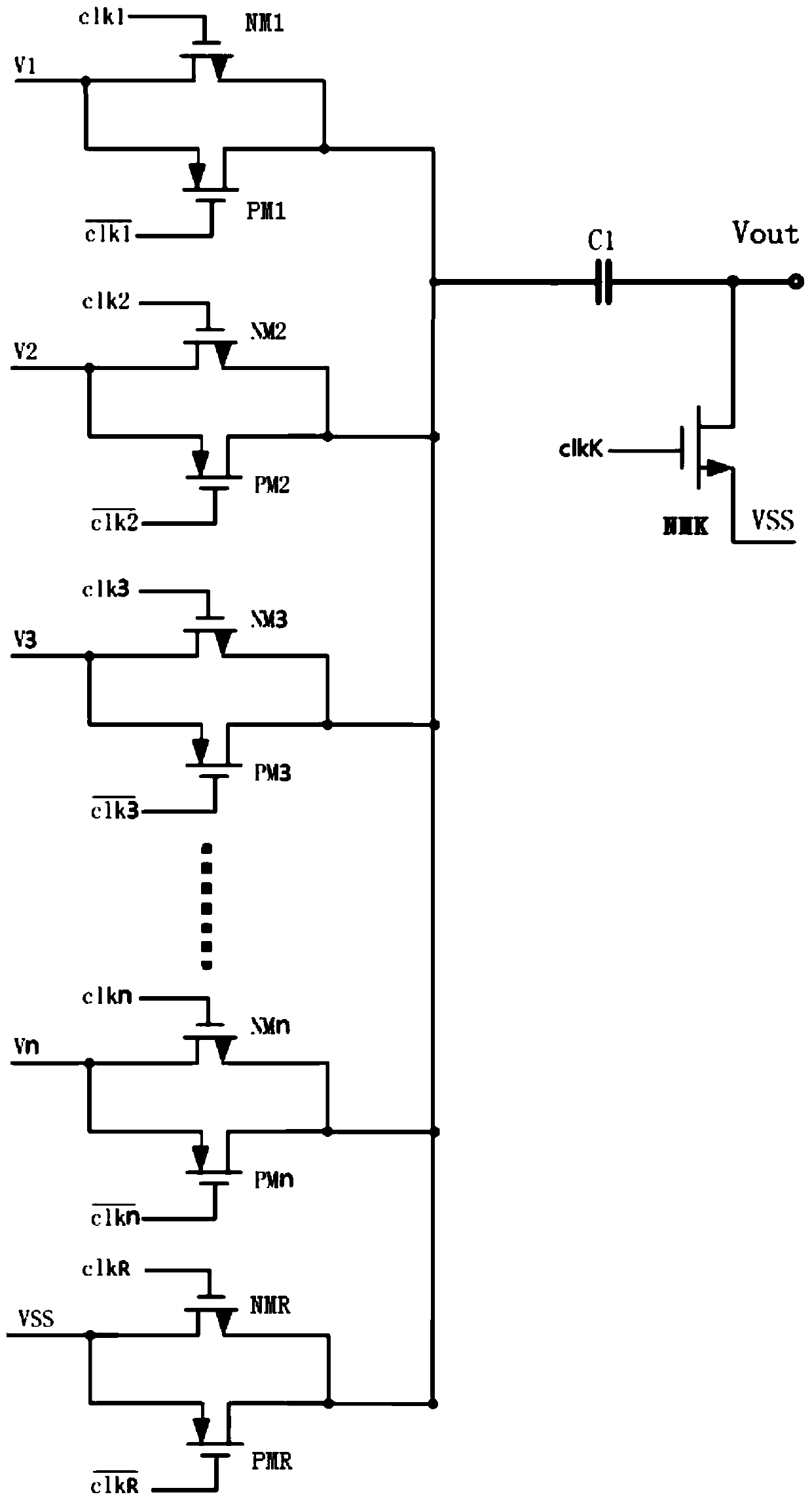
[0025] On the basis of Embodiment 1, a structure of gate expansion is provided, such as image 3 shown. A plurality of gating units with the same structure are added, each gating unit is respectively connected to a voltage to be sampled, and the output terminals of all gating units are connected to the sampling capacitor C1 at a common point.

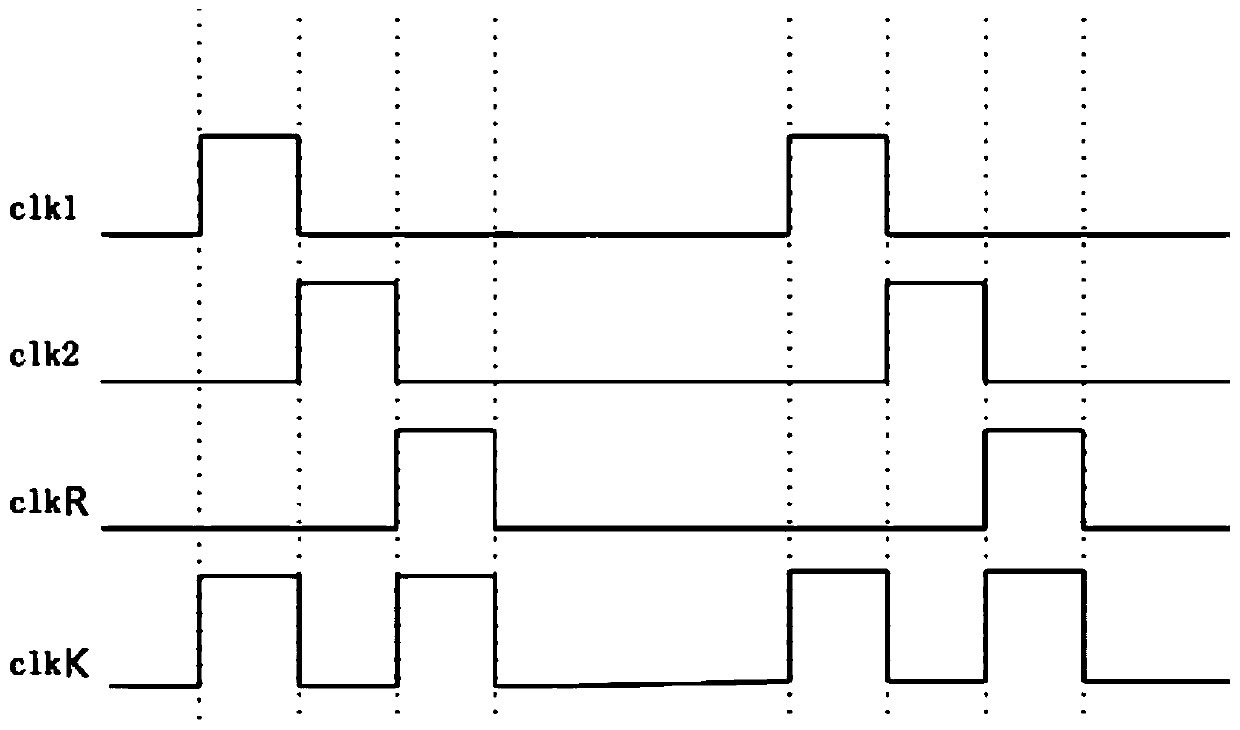
[0026] By rationally configuring the clock signal, two different voltages to be sampled can be combined arbitrarily and the difference voltage between the two can be obtained for output. if used as Figure 4 The clock signal shown is taken as an example. First, as in the working process of the first embodiment, the differential output of V2-V1 and the reset work are completed in the first to third time sequence intervals. Then complete the V3-V2 differential output and reset work again in the fifth to seventh timing intervals. Finally, Vn-V is completed in the ninth to eleventh timing intervals n-1 differential output and its reset ...


PUM


Abstract

The invention discloses a multichannel voltage difference value sampling circuit and method, relates to a new generation of information technology, and aims to solve the problems of high circuit powerconsumption, complicated circuit and high requirement for the loop stability in the prior art. The sampling circuit comprises more than two gating units, a reset unit, a sampling capacitor and a switch unit. The control ends of the gating units are respectively connected with gating signals one by one, and the input ends of the gating units are respectively connected with each to-be-sampled voltage one by one; the output ends of all the gating units and the output end of the reset unit are connected and then are connected with the sampling capacitor and the switch unit in series. The samplingcircuit and method have the advantages that charge distribution of the sampling capacitor can be reconfigured by reasonably switching on the gating unit and the switch unit, voltage difference can besampled needless of an operational amplifier, the circuit structure is very simple and can be expanded infinitely, two or more voltages can be randomly combined for sampling, and the adaptability isvery high.

Description

technical field [0001] The invention relates to a new generation of information technology, in particular to a multi-channel voltage difference sampling circuit and a sampling method thereof, especially for branch voltage difference sampling. Background technique [0002] In processing voltage signals, it is often necessary to sample the voltage difference between two points in the circuit and output a difference level. For this type of circuit, subtraction circuits built with operational amplifiers are more commonly used. This type of circuit consumes a lot of power and needs to pay attention to the stability of the loop. As an energy storage element, capacitors are often used in sampling schemes, and are mostly used in sample-and-hold circuits, but the circuits in the solution of differential (differential) voltage sampling are relatively cumbersome. Contents of the invention [0003] In order to solve the above-mentioned problems in the prior art, the purpose of the pr...

Claims


Application Information

Patent Timeline
Patent Type & Authority Applications(China)
IPC IPC(8): G01R19/10
CPCG01R19/10
Inventor 陈志坚陈鸿李斌郑彦祺吴朝晖
Owner SOUTH CHINA UNIV OF TECH
Why Eureka
Try Eureka