Method for removing polymer

A polymer and physical technology, applied in electrical components, semiconductor/solid-state device manufacturing, circuits, etc., can solve problems affecting the structural performance of pads

Active Publication Date: 2019-12-20
SHANGHAI HUALI MICROELECTRONICS CORP
View PDF10 Cites 1 Cited by
  • Summary
  • Abstract
  • Description
  • Claims
  • Application Information

AI Technical Summary

Problems solved by technology

[0005] The purpose of the present invention is to provide a polymer removal method to solve th

Method used


Image

  • Method for removing polymer
  • Method for removing polymer
  • Method for removing polymer

Examples


Embodiment Construction

[0033] The polymer removal method proposed in the present invention will be further described in detail below in conjunction with the accompanying drawings and specific examples. The advantages and features of the present invention will be more apparent from the following description. It should be noted that all the drawings are in a very simplified form and use imprecise scales, and are only used to facilitate and clearly assist the purpose of illustrating the embodiments of the present invention.

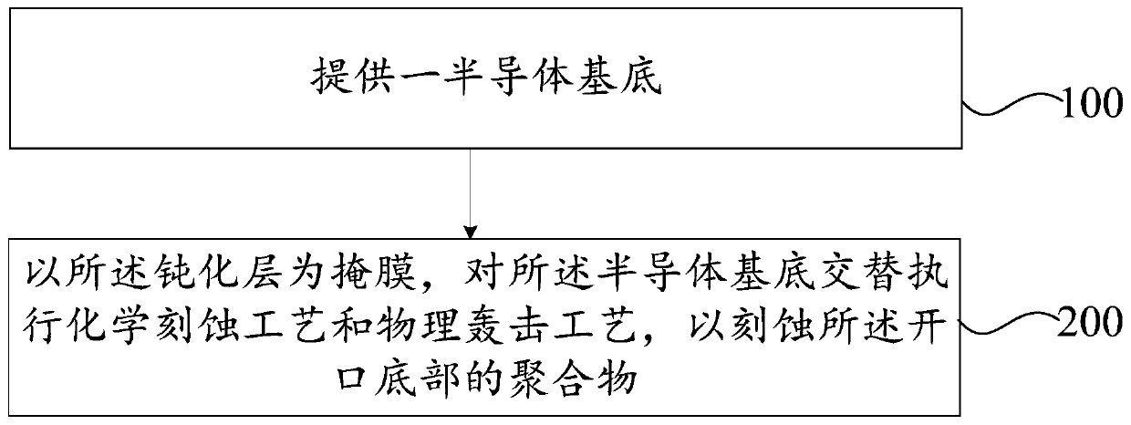
[0034] figure 1 It is a schematic flow diagram of a polymer removal method according to an embodiment of the present invention, such as figure 1 Shown, the removal method of described polymer comprises:

[0035] Step 100, providing a semiconductor substrate.

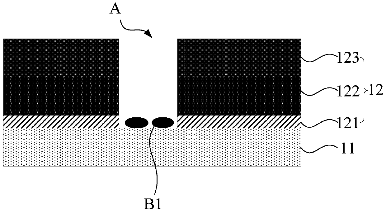
[0036] The semiconductor substrate can be as figure 2 As shown, the semiconductor substrate may include a top layer metal layer 11 and a passivation layer 12 formed overlappingly, and the semiconductor substrate further...


PUM


Abstract

The invention provides a method for removing a polymer. The method comprises a step of providing a semiconductor substrate, wherein the semiconductor substrate comprises a top metal layer and a passivation layer which are formed in an overlapped mode, an opening is formed in the passivation layer, the opening penetrates through the passivation layer to expose the top metal layer, and the polymer is left at a bottom of the opening, a step of alternately executing a chemical etching process and a physical bombardment process on the semiconductor substrate by taking the passivation layer as a mask so as to etch the polymer at the bottom of the opening. The method for removing the polymer provided by the invention is relatively high in speed, other parts of the semiconductor substrate can be prevented from being damaged, and the performance of the semiconductor substrate is ensured.

Description

technical field [0001] The invention relates to the technical field of semiconductors, in particular to a polymer removal method. Background technique [0002] In the technical field of semiconductor manufacturing, a pad structure is usually prepared on a semiconductor wafer, so that the subsequent bonding of the semiconductor wafer and other components can be realized based on the pad structure. Wherein, in the process of preparing the pad structure, the top metal layer is usually formed first, then a passivation layer is formed on the top metal layer, and the passivation layer is etched to form an opening to expose the top layer The metal layer, and then lead out the top metal layer by filling the opening with a conductive material to form a pad structure. However, usually, after the opening is formed by etching the passivation layer, a fluorine-containing polymer will remain at the bottom of the opening, and the fluorine ions will react with the metal on the surface of t...

Claims


Application Information

Patent Timeline
IPC IPC(8): H01L21/3105H01L21/311H01L21/48
CPCH01L21/31058H01L21/31138H01L21/31144H01L21/4828
Inventor 孙文彦王一许鹏凯
Owner SHANGHAI HUALI MICROELECTRONICS CORP
Why Eureka
Try Eureka