A split gate cstbt with pmos current clamping and method of making the same

A separation gate and current technology, which is applied in the field of separation gate CSTBT and its production, can solve the problems of excessive saturation current, degradation of breakdown characteristics of CSTBT, etc., to improve saturation current, improve short-circuit safety working ability, and improve carrier distribution Effect

Active Publication Date: 2020-12-29
UNIV OF ELECTRONICS SCI & TECH OF CHINA
View PDF5 Cites 0 Cited by
  • Summary
  • Abstract
  • Description
  • Claims
  • Application Information

AI Technical Summary

Problems solved by technology

[0004] In order to improve the impact of the introduction of the carrier storage layer on the degradation of the breakdown characteristics of the CSTBT and the shortcomings of excessive saturation current during forward conduction, the present invention proposes a split-gate CSTBT structure with PMOS current clamping, such as figure 2 shown

Method used


Image

  • A split gate cstbt with pmos current clamping and method of making the same
  • A split gate cstbt with pmos current clamping and method of making the same
  • A split gate cstbt with pmos current clamping and method of making the same

Examples


Embodiment 1

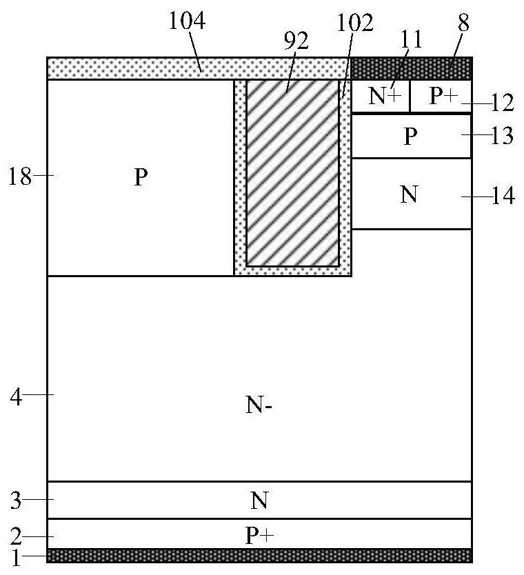
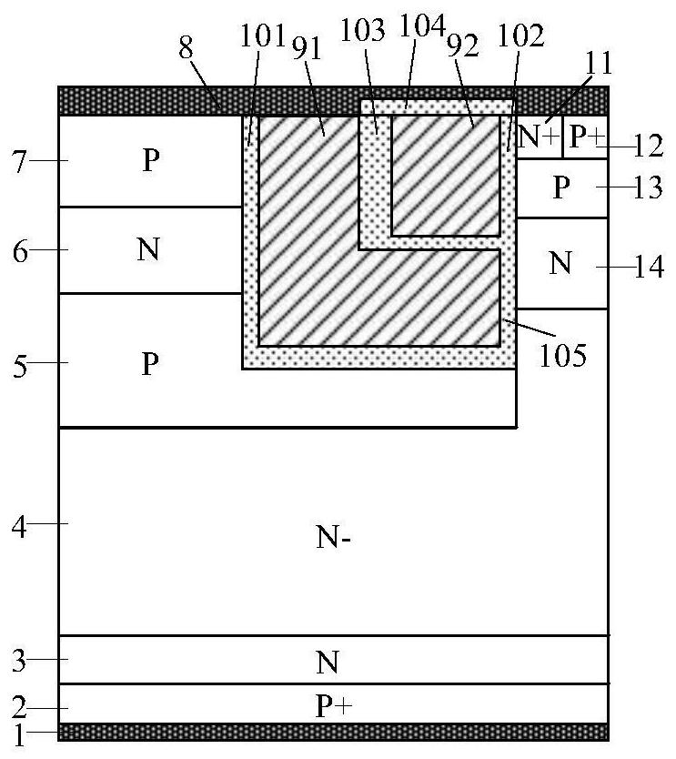
[0053] A split-gate CSTBT with PMOS current clamping, its half-cell structure is as follows figure 2 As shown, it includes: back collector metal 1, P-type collector region 2 located on and connected to the back collector metal 1, N-type field stop layer 3 located on and connected to the P-type collector region 2 and An N-drift region 4 located on and connected to the N-type field stop layer 3; a P-type buried layer 5 located on and connected to the N-drift region 4 and an N-type charge located on and connected to the N-drift region 4 Storage layer 14; N-type doped layer 6 located on the top of the P-type buried layer and connected to it; P-type doped layer 7 located on the top of the N-type doped layer 6 and connected to it; located on the top of the N-type charge storage layer and connected to it The P-type base region 13; the N+ emitter region 11 and the P+ emitter region 12 that are independent of each other and placed side by side on the top of the P-type base region; Th...

Embodiment 2

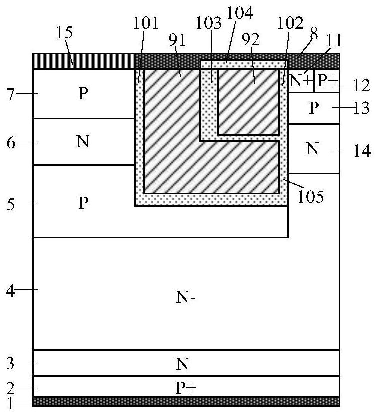
[0055] A split-gate CSTBT with PMOS current clamping, its half-cell structure is as follows image 3 As shown, this embodiment introduces a Schottky contact metal 15 connected to the P-type doped region 7 on the basis of the first embodiment, and the rest of the structure is the same as that of the first embodiment.

[0056] The Schottky contact metal 15 introduced in this embodiment has the same potential as the emitter metal 1 , and the introduction of the Schottky contact metal 15 can reduce the conduction voltage drop of the PMOS and reduce the switching loss of the device.

Embodiment 3

[0058] A CSTBT with a PMOS current clamping separation gate, and its half-cell structure is as follows Figure 4 As shown, in this embodiment, on the basis of embodiment 1, the P-type buried layer 5 is extended below the N-type charge storage layer 14, and the rest of the structure is the same as that of embodiment 1.

[0059] In this embodiment, the purpose of extending the P-type buried layer 5 to the bottom of the N-type charge storage layer 14 is that when the mesa of the structure increases, the P-type buried layer 5 can still transfer the drift region below the N-type charge storage layer 14 to the bottom of the N-type charge storage layer 14. depletion, so that the potential of the N-type charge storage layer 14 is determined by the potential of the P-type buried layer 5, and the structure can reduce the saturation current by adjusting the concentration of the P-type buried layer.


PUM

PropertyMeasurementUnit
thicknessaaaaaaaaaa

Abstract

The invention belongs to the technical field of a power semiconductor device and relates to a split gate CSTBT with PMOS current clamping and a manufacturing method of the split gate CSTBT. A PMOS structure is introduced on the basis of a traditional CSTBT, a saturation current during forward conduction of a device is effectively improved, the short-circuit safe working capability of the device isimproved, moreover, the influence of an N-type charge storage layer 14 on the breakdown characteristic of the device is eliminated, therefore, the doping concentration of the N-type charge storage layer 14 can be improved to improve carrier distribution during forward conduction of the device, so the conductivity modulation capability of a drift region is improved, forward conduction voltage dropof the device is reduced, the gate capacitance, especially the Miller capacitance, of the device is reduced by an L-shaped separated gate structure, the switching speed of the device is improved, switching loss of the device is reduced, since a separation gate and the gate structure are integrated in the same groove, the area of a chip is saved.

Description

technical field [0001] The invention belongs to the technical field of power semiconductor devices, and relates to a split gate CSTBT with PMOS current clamping and a manufacturing method thereof. Background technique [0002] Insulated gate bipolar transistor (IGBT) combines the advantages of field effect transistor (MOSFET) and bipolar crystalline transistor (BJT). It has the advantages of high state current density, low conduction voltage, low loss and good stability. Therefore, it has developed into one of the core electronic components in modern power electronic circuits, and is widely used in various fields such as transportation, communication, household appliances and aerospace. The use of IGBT has greatly improved the performance of power electronic systems. [0003] Since the IGBT was invented in the 1980s, the IGBT has been developing along the trend of reducing device switching loss, increasing device operating frequency and improving device reliability. IGBT ...

Claims


Application Information

Patent Timeline
Patent Type & Authority Patents(China)
IPC IPC(8): H01L29/06H01L29/423H01L29/739H01L21/28H01L21/331
CPCH01L29/0684H01L29/401H01L29/42312H01L29/66348H01L29/7397H01L29/7398
Inventor 张金平王康赵阳刘竞秀李泽宏张波
Owner UNIV OF ELECTRONICS SCI & TECH OF CHINA
Why Eureka
Try Eureka