Split gate TIGBT with self-biased PMOS and manufacturing method thereof

A separation gate, self-biasing technology, applied in semiconductor/solid-state device manufacturing, electrical components, circuits, etc., can solve the problems of unfavorable device miniaturization development, affecting device stability, uneven current distribution on the device surface, etc. The effect of short-circuit safe working ability, saving area and improving conductance modulation ability

Active Publication Date: 2019-11-19
UNIV OF ELECTRONICS SCI & TECH OF CHINA
View PDF4 Cites 1 Cited by
  • Summary
  • Abstract
  • Description
  • Claims
  • Application Information

AI Technical Summary

Problems solved by technology

However, the reduction of channel density leads to uneven distribution of current on the surface of the device, which affects the stability of the normal operation of the device, and the reduction of channel density is not conducive to the development of device miniaturization

Method used


Image

  • Split gate TIGBT with self-biased PMOS and manufacturing method thereof
  • Split gate TIGBT with self-biased PMOS and manufacturing method thereof
  • Split gate TIGBT with self-biased PMOS and manufacturing method thereof

Examples


Embodiment 1

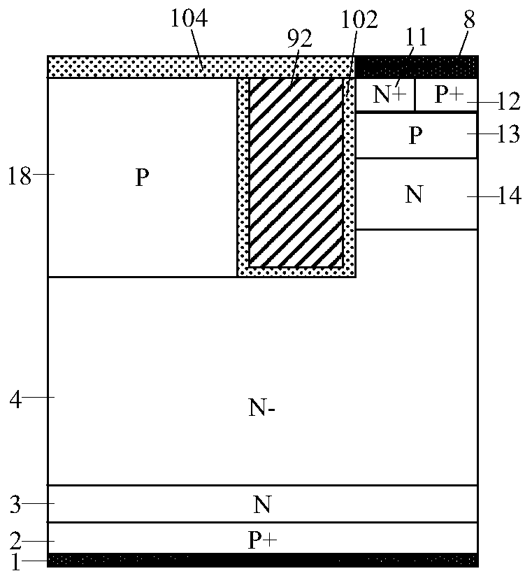
[0054] A split-gate TIGBT with self-biased PMOS, whose half-cell structure is as figure 2 As shown, it includes: back collector metal 1, P-type collector region 2 located on and connected to the back collector metal 1, N-type field stop layer 3 located on and connected to the P-type collector region 2 and The N-drift region 4 located on and connected to the N-type field stop layer 3; the P-type buried layer 5 located on the top of the N-drift region 4 and connected to it, and the P-type base layer located on and connected to the N-drift region 4 Region 13; the N-type doped layer 6 located on the top of the P-type buried layer and connected to it; the P-type doped layer 7 located on the top of the N-type doped layer 6 and connected to it; the upper part of the P-type base region 13 is independent and side by side Placed N+ emitter region 11 and P+ emitter region 12; located on the top of the P-type buried layer 5, the side walls of the N-type doped layer 6, the side walls of th...

Embodiment 2

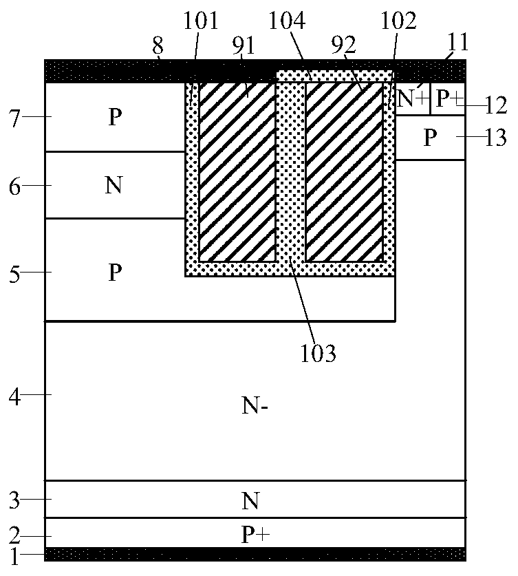
[0056] A split-gate TIGBT with self-biased PMOS, whose half-cell structure is as image 3 As shown, it includes: back collector metal 1, P-type collector region 2 located on and connected to the back collector metal 1, N-type field stop layer 3 located on and connected to the P-type collector region 2 and The N-drift region 4 located on and connected to the N-type field stop layer 3; the P-type buried layer 5 and the N-type charge storage layer 14 located on the upper part of the N-drift region 4 and connected to it; located on the upper part of the N-type charge storage layer The P-type base region 13 connected to it; the N-type doped layer 6 located on the top of the P-type buried layer and connected to it; the P-type doped layer 7 located on the top of the N-type doped layer 6 and connected to it; The N+ emitter region 11 and the P+ emitter region 12 that are independent and placed side by side in the upper part of the region 13; located on the upper part of the P-type buri...

Embodiment 3

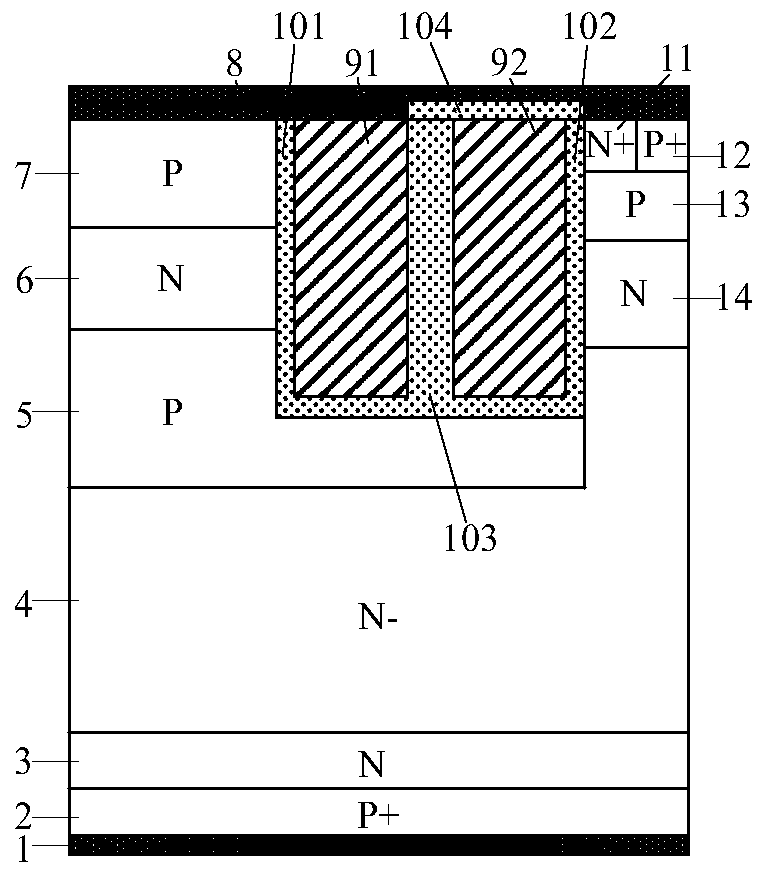
[0058] A split-gate TIGBT with self-biased PMOS, whose half-cell structure is as Figure 4 As shown, this embodiment introduces a Schottky contact metal 15 connected to the P-type doped region 7 on the basis of embodiment 1, and the rest of the structure is the same as that of embodiment 2.

[0059] The Schottky contact metal 15 introduced in this embodiment has the same potential as the emitter metal 1 , and the introduction of the Schottky contact metal 15 can reduce the conduction voltage drop of the PMOS and reduce the switching loss of the device.


PUM


Abstract

The invention belongs to the technical field of power semiconductor devices and relates to a split gate TIGBT with a self-biased PMOS and a manufacturing method thereof. By introducing a PMOS structure on the basis of a traditional TIGBT, the saturation current is improved during the forward conduction of a device and the short-circuit safe operation capability of the device is improved without adecrease in channel density. An extra current discharge path provided by the PMOS structure increases the speed of the device for extracting holes in an off state, thereby increasing the switching speed of the device and reducing the switching loss of the device. In addition, for a TIGBT with an N-type charge storage layer, a P-type buried layer can shield the impact of the N-type charge storage layer on the breakdown characteristics of the device, so the doping concentration of the N-type charge storage layer can be increased to further improve the carrier distribution of the device during forward conduction, improve the conductance modulation capability of a drift region, and further improve the compromise between the forward voltage drop Vce (on) of the device and the turn-off loss Eofconductance.

Description

technical field [0001] The invention belongs to the technical field of power semiconductor devices, and relates to a split-gate TIGBT with self-biased PMOS and a manufacturing method thereof. Background technique [0002] Insulated gate bipolar transistor (IGBT), as one of the core electronic components in modern power electronic circuits, is widely used in various fields such as transportation, communication, household appliances, and aerospace. The insulated gate bipolar transistor is a new type of power electronic device composed of an insulated field effect transistor (MOSFET) and a bipolar junction transistor (BJT), which can be equivalent to a MOSFET driven by a bipolar junction transistor. The IGBT combines the MOSFET structure and the working mechanism of the bipolar junction transistor. It not only has the advantages of easy driving, low input impedance, and fast switching speed of the MOSFET, but also has the advantages of large on-state current density, low conduc...

Claims


Application Information

Patent Timeline
Patent Type & Authority Applications(China)
IPC IPC(8): H01L29/06H01L21/331H01L29/739
CPCH01L29/0684H01L29/66348H01L29/7397H01L29/7398
Inventor 张金平王康赵阳刘竞秀李泽宏张波
Owner UNIV OF ELECTRONICS SCI & TECH OF CHINA
Why Eureka
Try Eureka