GaN device structure and preparation method thereof

A device structure and composite structure technology, applied in semiconductor devices, electrical components, transistors, etc., can solve problems such as field plate damage, GaN device ohmic contact is difficult to effectively improve, etc., to avoid damage, high reliability, and improve doping concentration. Effect

Active Publication Date: 2021-07-09
浙江集迈科微电子有限公司
View PDF12 Cites 0 Cited by
  • Summary
  • Abstract
  • Description
  • Claims
  • Application Information

AI Technical Summary

Problems solved by technology

[0005] In view of the shortcomings of the prior art described above, the purpose of the present invention is to provide a GaN device structure and its preparation method, which are used to solve the problems in the prior art that the ohmic contact of GaN devices is difficult to be effectively improved and the field plate preparation is easy to cause damage, etc.

Method used


Image

  • GaN device structure and preparation method thereof
  • GaN device structure and preparation method thereof
  • GaN device structure and preparation method thereof

Examples


Embodiment 1

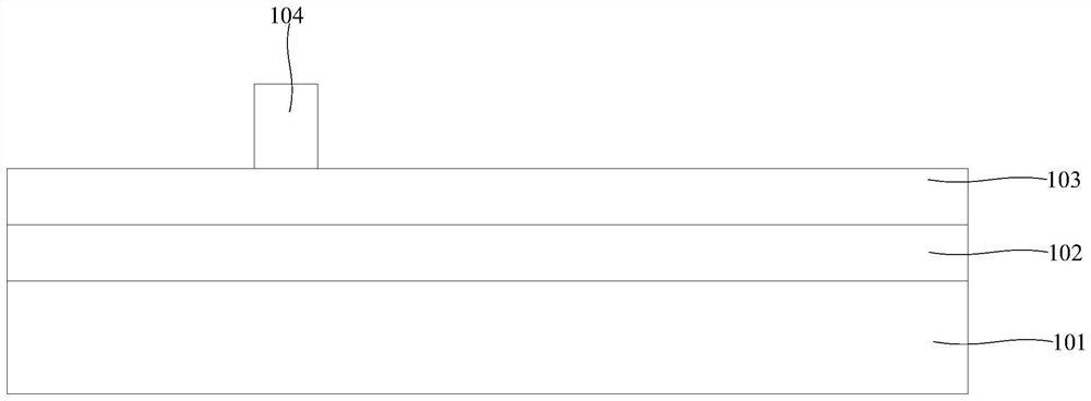
[0065] Such as figure 1 Shown, the present invention provides a kind of preparation method of GaN device structure, and described preparation method comprises the following steps:

[0066] S1, providing a substrate, and preparing an epitaxial structure on the substrate, the epitaxial structure at least including a GaN channel layer and an initial barrier layer on the GaN channel layer;

[0067] S2, preparing a gate auxiliary structure on the epitaxial structure to define a gate region;

[0068] S3, preparing a doped barrier composite structure and a gate step-assisted composite structure on the epitaxial structure, the doped barrier composite structure includes the first epitaxial doped barrier layer to the first epitaxial doped barrier layer formed sequentially from bottom to top The barrier layer is epitaxially doped N times, and the gate step auxiliary composite structure includes a first gate step auxiliary structure to an Mth gate step auxiliary structure;

[0069] Wher...


PUM

PropertyMeasurementUnit
thicknessaaaaaaaaaa
thicknessaaaaaaaaaa
thicknessaaaaaaaaaa

Abstract

The invention provides a GaN device structure and a preparation method thereof, and the preparation method comprises the steps: preparing a GaN channel layer and an initial barrier layer on a substrate, preparing a gate region auxiliary structure, and preparing a doped barrier composite structure and a gate step auxiliary composite structure, wherein the gate step auxiliary composite structure penetrates through the doped barrier composite structure in a step shape, and each stage of gate step auxiliary structure gradually rises in the direction from the gate region to the drain electrode; removing the gate region auxiliary structure and the gate step auxiliary composite structure; preparing a source electrode and the drain electrode, and preparing a gate composite structure. By introducing the doped barrier composite structure, based on the gate region auxiliary structure and the gate step auxiliary structure, through multiple selective epitaxy, the doping concentration can be improved, and a low ohmic contact electrode can be realized; and through designing the stepped gate and the gate field plate, a stepped drain field plate can be further designed at the same time, the 2DEG concentration can be controlled, damage caused by the etching process is avoided, and the reliability is high.

Description

technical field [0001] The invention belongs to the technical field of semiconductor device manufacturing, and in particular relates to a GaN device structure and a preparation method thereof. Background technique [0002] The research and application of GaN materials is the frontier and hotspot of global semiconductor research at present. It is a new type of semiconductor material for the development of microelectronic devices and optoelectronic devices. The third generation of semiconductor materials after semiconductor materials. It has properties such as wide direct band gap, strong atomic bond, high thermal conductivity, good chemical stability (hardly corroded by any acid) and strong radiation resistance. [0003] However, with the development and demand of technology, it is difficult to effectively improve the ohmic contact of the electrode in the GaN device structure. In addition, the formation of the gate field plate and the drain field plate in the existing proces...

Claims


Application Information

Patent Timeline
Patent Type & Authority Applications(China)
IPC IPC(8): H01L29/10H01L29/20H01L29/06H01L29/78
CPCH01L29/1029H01L29/2003H01L29/0603H01L29/0684H01L29/78
Inventor 马飞邹鹏辉左亚丽朱伟超
Owner 浙江集迈科微电子有限公司
Why Eureka
Try Eureka