Zirconium disulfide-germanium nano-pyramid heterojunction, preparation method and application thereof

A technology of zirconium disulfide and pyramid structure, which is applied in the manufacture of final products, sustainable manufacturing/processing, photovoltaic power generation, etc., can solve the problems of insufficient light absorption and low photoelectric conversion efficiency, and achieves improved light absorption and photoelectric conversion efficiency. , to achieve the effect of wide-angle absorption

Inactive Publication Date: 2019-12-20
ANYANG NORMAL UNIV
View PDF0 Cites 2 Cited by
  • Summary
  • Abstract
  • Description
  • Claims
  • Application Information

AI Technical Summary

Problems solved by technology

[0003] In view of the deficiencies in the prior art, the present invention proposes a zirconium disulfide-germanium nano-pyramid heterojunction, a preparation method and its application, aiming at overcoming the occurrence of existing heterojunctions based on two-dimensional materials in the application process of optoelectronic devices Insufficient light absorption and low photoelectric conversion efficiency, broaden the structure and types of heterojunctions based on two-dimensional materials

Method used


Image

  • Zirconium disulfide-germanium nano-pyramid heterojunction, preparation method and application thereof

Examples


Embodiment 1

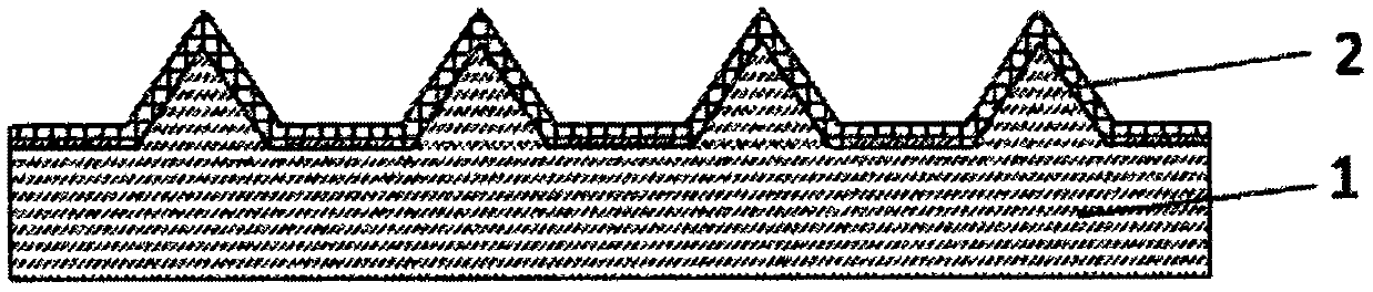
[0021] refer to figure 1 , the invention includes a layer of germanium substrate, and the zirconium disulfide thin film is arranged on the germanium substrate. In this embodiment, the germanium substrate adopts a 1×1cm substrate with a thickness of 150 μm 2 single-sided polished single-crystal germanium sheet, the conductivity type is n-type, and the resistivity is 0.05Ωcm; the polished surface of the germanium substrate is etched by an anisotropic etching method to etch a pyramid structure with a quadrilateral base, and the side length of the quadrilateral base is is 0.5 μm, the height of the pyramid structure is 0.5 μm, and the density of the nano-pyramids on the surface of the germanium sheet is 4×10 8 cm -2 . In this embodiment, the zirconium disulfide film evenly covers the surface of the germanium substrate and the sidewalls of the nano-pyramids, and the thickness of the zirconium disulfide film is 12 nm.

[0022] The preparation steps of the heterojunction in this e...

Embodiment 2

[0029] refer to figure 1 , the invention includes a layer of germanium substrate, and the zirconium disulfide thin film is arranged on the germanium substrate. In this embodiment, the germanium substrate adopts a 2×1cm substrate with a thickness of 150 μm 2 A single-sided polished single-crystal germanium wafer, the conductivity type is n-type, and the resistivity is 0.2Ωcm; the polished surface of the germanium substrate is etched by an anisotropic etching method to etch a pyramid structure with a quadrilateral base, and the side length of the quadrilateral base is is 2 μm, the height of the pyramid structure is 2 μm, and the density of the nano-pyramids on the surface of the germanium sheet is 4×10 7 cm -2 . In this embodiment, the zirconium disulfide film evenly covers the surface of the germanium substrate and the side walls of the nano-pyramids, and the thickness of the zirconium disulfide film is 48 nm.

[0030] The preparation steps of the heterojunction in this emb...

Embodiment 3

[0037] refer to figure 1 , the invention includes a layer of germanium substrate, and the zirconium disulfide thin film is arranged on the germanium substrate. In this embodiment, the germanium substrate adopts a 2×2cm substrate with a thickness of 200 μm 2 single-sided polished single-crystal germanium sheet, the conductivity type is n-type, and the resistivity is 0.25Ωcm; the polished surface of the germanium substrate is etched by an anisotropic etching method to etch a pyramid structure with a quadrilateral base, and the side length of the quadrilateral base is is 5 μm, the height of the pyramid structure is 5 μm, and the density of the nano-pyramids on the surface of the germanium sheet is 4×10 6 cm -2 . In this embodiment, the zirconium disulfide film uniformly covers the surface of the germanium substrate and the side walls of the nano-pyramids, and the thickness of the zirconium disulfide film is 60 nm.

[0038] The preparation steps of the heterojunction in this e...


PUM

PropertyMeasurementUnit
thicknessaaaaaaaaaa
thicknessaaaaaaaaaa
heightaaaaaaaaaa

Abstract

The invention discloses a zirconium disulfide-germanium nano-pyramid heterojunction, a preparation method and an application thereof. The zirconium disulfide-germanium nano-pyramid heterojunction includes a single-side polished monocrystalline germanium wafer with nano-pyramid structure on the surface. A layer of uniform and continuous zirconium disulfide film is arranged on the monocrystalline germanium wafer. The method for preparing the heterojunction according to the present invention comprises the anisotropic etching of the surface of the germanium wafer and the zirconium disulfide preparation by atomic layer deposition. Since the heterojunction of the present invention is a combination of a novel two-dimensional semiconductor zirconium disulfide and a germanium substrate with a three-dimensional nanostructure on the surface, not only can the advantages of the novel two-dimensional material be exerted, but also the light absorption wavelength can be adjusted and the light absorption effect can be enhanced. Further, the atomic layer deposition process can make the zirconium disulfide film completely cover the surface of the germanium substrate and the side walls of the nano-pyramid to achieve comprehensive contact, so that the prepared heterojunction region has large area, thereby improving the photoelectric conversion efficiency of an optoelectronic device.

Description

Technical field: [0001] The invention relates to the field of two-dimensional material heterojunctions, in particular to a zirconium disulfide-germanium nano-pyramid heterojunction, a preparation method and an application thereof. Background technique: [0002] In recent years, the development and application of new two-dimensional materials have attracted great attention. The family of 2D materials is vast, and their properties vary. A heterojunction based on two-dimensional materials is composed of a variety of two-dimensional materials or non-two-dimensional materials with different physical properties. The heterojunction based on two-dimensional materials integrates the advantages of multiple materials, learns from each other, overcomes the defects of a single material, and even exerts novel characteristics that the original materials do not have due to the unique coupling mechanism between materials. It is expected to be used in optoelectronics. A major breakthrough h...

Claims


Application Information

Patent Timeline
Patent Type & Authority Applications(China)
IPC IPC(8): H01L31/0352H01L31/0336H01L31/074H01L31/109H01L31/18
CPCH01L31/0336H01L31/03529H01L31/074H01L31/109H01L31/18Y02E10/50Y02P70/50
Inventor 张希威孟丹汤振杰
Owner ANYANG NORMAL UNIV
Why Eureka
Try Eureka