Waveguide structure, optical device and method for manufacturing waveguide structure

A technology of waveguide structure and fabrication method, applied in the field of optical communication, can solve the problems of intrinsic loss, reduce the performance of femtosecond lasers, etc., and achieve the effects of reducing intrinsic loss, increasing complexity, and reducing damage

Inactive Publication Date: 2019-12-20
WUHAN OPTICAL VALLEY INFORMATION OPTOELECTRONICS INNOVATION CENT CO LTD
View PDF3 Cites 4 Cited by
  • Summary
  • Abstract
  • Description
  • Claims
  • Application Information

AI Technical Summary

Problems solved by technology

In related technologies, while changing the modulation depth of femtosecond lasers, intrinsic loss will be introduced, reducing the performance of femtosecond lasers

Method used


Image

  • Waveguide structure, optical device and method for manufacturing waveguide structure
  • Waveguide structure, optical device and method for manufacturing waveguide structure
  • Waveguide structure, optical device and method for manufacturing waveguide structure

Examples


Embodiment Construction

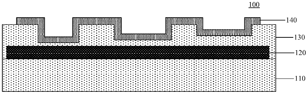
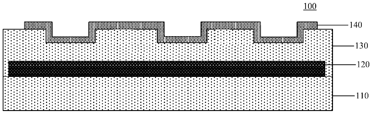
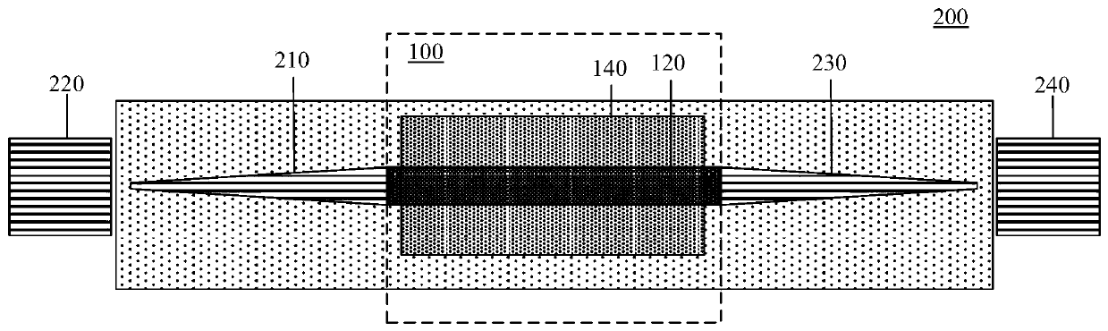
[0046] The technical solutions of the present invention will be further described in detail below in conjunction with the drawings and embodiments. Although exemplary embodiments of the present disclosure are shown in the drawings, it should be understood that the present disclosure may be embodied in various forms and should not be limited by the embodiments set forth herein. Rather, these embodiments are provided for more thorough understanding of the present disclosure and to fully convey the scope of the present disclosure to those skilled in the art.

[0047] In the following paragraphs the invention is described more specifically by way of example with reference to the accompanying drawings. Advantages and features of the present invention will be apparent from the following description and claims. It should be noted that all the drawings are in a very simplified form and use imprecise scales, and are only used to facilitate and clearly assist the purpose of illustratin...


PUM


Abstract

Embodiments of the present invention disclose a waveguide structure, an optical device, and a method for manufacturing the waveguide structure. The waveguide structure comprises: a first dielectric layer; a core layer stacked on the first dielectric layer, wherein the refractive index of the core layer is greater than the refractive index of the first dielectric layer; a second dielectric layer stacked on the core layer, wherein the second dielectric layer comprises a groove, the opening of the groove faces away from the core layer, and the refractive index of the second dielectric layer is smaller than the refractive index of the core layer; and an absorption layer covering the outer surface of the second dielectric layer, wherein the absorption layer is in contact with the side wall of the groove and the bottom of the groove, and the absorption layer has a non-linear saturation absorption property.

Description

technical field [0001] The embodiments of the present invention relate to the technical field of optical communication, and in particular, to a waveguide structure, an optical device, and a manufacturing method of the waveguide structure. Background technique [0002] Femtosecond lasers are one of the core devices in the field of optical communication technology, which can generate femtosecond-level pulsed light sources with a wide range of applications. Chip-scale femtosecond lasers based on nonlinear saturable absorbers can form ultrashort pulses, and have the advantages of high stability and small size. In the related art, when the modulation depth of the femtosecond laser is changed, intrinsic loss will be introduced to reduce the performance of the femtosecond laser. Contents of the invention [0003] In view of this, embodiments of the present invention provide a waveguide structure, an optical device, and a method for manufacturing the waveguide structure. [0004...

Claims


Application Information

Patent Timeline
Patent Type & Authority Applications(China)
IPC IPC(8): H01S3/11
CPCH01S3/1115
Inventor 胡晓肖希王磊张宇光陈代高李淼峰
Owner WUHAN OPTICAL VALLEY INFORMATION OPTOELECTRONICS INNOVATION CENT CO LTD
Why Eureka
Try Eureka