Spin orbit materials for efficient spin current generation

a technology of spin orbit and materials, applied in the field of spin torque devices, can solve the problems of high power consumption, hindering sot based applications, and proving problematic to integrate sot devices with cmos technology

Active Publication Date: 2019-02-21
NAT UNIV OF SINGAPORE
View PDF0 Cites 16 Cited by
  • Summary
  • Abstract
  • Description
  • Claims
  • Application Information

AI Technical Summary

Benefits of technology

[0008]An improved SOT device (e.g., a SOT-based MRAM, logic device, racetrack memory, etc.) is provided that replaces a traditional NM layer adjacent to a magnetic layer with a NM layer that includes one of three classes of materials, namely an CMOS-compatible composite (e.g., copper platinum (CuPt)) alloy, a topological insulator (TI) (e.g., bismuth selenide (Bi2Se3), bismuth selenium (BixSe1-x) alloy, bismuth antimony (Bi1-xSbx) alloy, etc.) or a TI / non-magnetic metal interface (e.g., a Bi2Se3 / silver (Ag), BixSe1-x / Ag, Bi1-xSbx / Ag, etc.) interface, that provide efficient current generation.

Problems solved by technology

As such, it has proved problematic to integrate SOT devices with CMOS technology.
Further, current density (JC) desired for SOT induced magnetization switching using HMs (such as Pt, Ta etc.) is high, e.g., in the order of approximately 107-108 A / cm2, which hinders SOT based applications.
The high value of JC causes high power consumption and necessitates a large current driving transistor.

Method used


Image

  • Spin orbit materials for efficient spin current generation
  • Spin orbit materials for efficient spin current generation
  • Spin orbit materials for efficient spin current generation

Examples


first embodiment

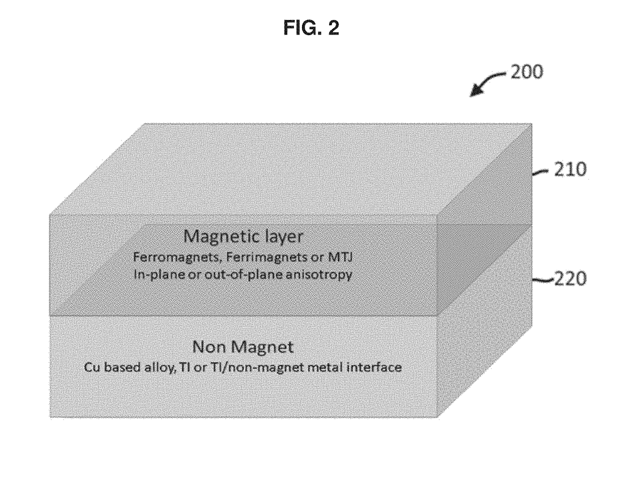
[0034]In a first embodiment, a SOT device replaces a traditional NM layer with a CMOS-compatible composite alloy (e.g., a Cu-based alloy such as CuPt alloy) NM layer that provides an extrinsic SHE mechanism. For example, in this embodiment, a SOT device may be structured as a stack that includes a substrate made of silicon (Si), a FM layer of permalloy (Py) (Ni8iFe19) (e.g., having a thickness of 5 nanometers (nm)), a CMOS compatible composite alloy NM layer made of Cu1-xPtx (e.g., having a thickness of 6 nm) where x (0-100%) is the atomic ratio of Pt in Cu1-xPtx alloy, a barrier layer of MgO (e.g., having a thickness of 1 nm), and a capping layer of SiO2 (e.g., having a thickness of 3 nm). The entire film stack may be deposited onto a thermally oxidized Si substrate at room temperature using magnetron sputtering. The composite alloy of Cu1-xPtx may be deposited by co-sputtering Cu and Pt targets. In order to tune the Pt concentration (x) in the Cu1-xPtx alloy, the sputtering power ...

second embodiment

[0057]In a second embodiment, a SOT device stack replaces a traditional NM layer with a topological insulator (TI) (e.g., Bi2Se3, BixSe1-x, Bi1-xSbx, etc.) NM layer. A large SOT may be generated using a TI (e.g., Bi2Se3, BixSe1-x, Bi1-xSbx, etc.) that may efficiently switch the magnetization of an adjacent FM layer with an extremely low JC. For example, in this embodiment, a SOT device may be structured as a stack that includes, a substrate (e.g., Al2O3), a TI NM layer (e.g., having a thickness of 5-20 QL, where 1 QL is approximately equal to 1 nm), a FM layer (e.g., CoFeB or NiFe, having a thickness of 7 nm), a barrier layer of MgO (e.g., having a thickness of 2 nm), and a capping layer of Al2O3 (e.g., having a thickness of 3 nm). The TI layer may be grown on the substrate using molecular beam epitaxy (MBE) or sputtering. The CoFeB layer and insulating capping layer may be sputtered onto the TI layer. The deposited films may be patterned using optical photolithography and Ar ion mi...

third embodiment

[0075]In a third embodiment, a SOT device stack replaces a traditional NM layer with a TI / non-magnetic metal interface (e.g., a Bi2Se3 / Ag, BixSe1-x / Ag, Bi1-xSbx / Ag, etc. interface) layer adjacent to the FM layer. A TI / non-magnetic metal interface (e.g., Bi2Se3 / Ag interface) Rashba effect can induce efficient charge-spin conversion. This Rashba interface may serve as a spin current source to achieve TI-based room temperature spin devices with high scalability and efficiency. For example, in one embodiment, a SOT device may be structured as a film stack that includes a substrate made of Al2O3, a Bi2Se3 / Ag interface layer (e.g., having a Bi2Se3 thickness of 10 QL where 1 QL is approximately equal to 1 nm, and an Ag thickness (tAg) up to 5 nm), a FM layer of Co40Fe40B20 (e.g., having a thickness of 7 nm), a barrier layer of MgO (e.g., having a thickness of 2 nm), and a capping layer of SiO2 (e.g., having a thickness of 4 nm).

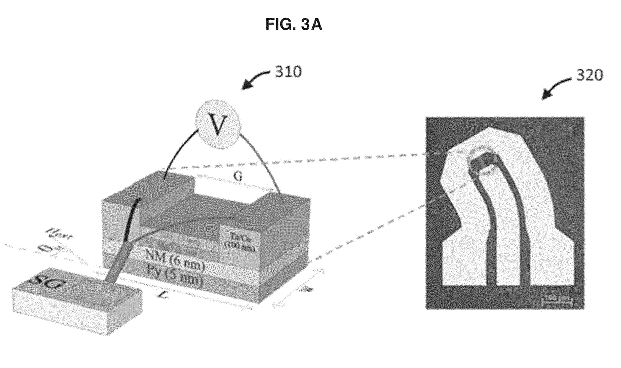
[0076]B. An Example Test Device and In-Plane Torque / Out-of-Pla...


PUM


Abstract

In one embodiment, a SOT device is provided that replaces a traditional NM layer adjacent to a magnetic layer with a NM layer that is compatible with CMOS technology. The NM layer may include a CMOS-compatible composite (e.g., CuPt) alloy, a TI (e.g., Bi2Se3, BixSe1-x, Bi1-xSbx, etc.) or a TI/non-magnetic metal (e.g., Bi2Se3/Ag, BixSe1-x/Ag, Bi1-xSbx/Ag, etc.) interface, that provides efficient spin current generation. Spin current may be generated in various manners, including extrinsic SHE, TSS or Rashba effect.

Description

RELATED APPLICATIONS[0001]The present application claims priority to Singapore Patent Application No. 10201706699P, titled “Spin Orbit Materials for Efficient Spin Current Generation,” filed by Applicant National University of Singapore on Aug. 16, 2017, the contents of which are incorporated by reference herein in their entirety.BACKGROUNDTechnical Field[0002]The present disclosure relates generally to spin torque devices and more specifically to a spin-orbit torque (SOT) based magnetic devices (“SOT devices”) and materials that may enable efficient spin current generation therein.Background Information[0003]Spin torque devices, such as spin torque magnetic random access memory (MRAMs), magnetic logic devices, racetrack memories, etc., manipulate magnetization directions to store information or for other purposes. Magnetization direction may be manipulated using current-induced STT. STT techniques have advanced over a number of years, and STT MRAMs is becoming commercially availabl...

Claims


Application Information

Patent Timeline
Patent Type & Authority Applications(United States)
IPC IPC(8): H01L43/10H01L43/06H01L27/22H01L43/04G11C11/16H03K19/18G11C19/08
CPCH01L43/10H01L43/065H01L27/222H01L43/04G11C11/161H03K19/18G11C19/0841G11C11/18G11C11/1675H10N50/00H10N50/85H10B61/00H10N52/80H10N52/101
Inventor RAMASWAMY, RAJAGOPALANWANG, YISHI, SHUYUANYANG, HYUNSOO
Owner NAT UNIV OF SINGAPORE
Why Eureka
Try Eureka