Epitaxial structure and low on-voltage transistor

An epitaxial structure and transistor technology, which is applied in the direction of semiconductor devices, circuits, electrical components, etc., can solve the problems of large turn-on voltage of transistors, difficulty in reducing, and high power consumption of devices, and achieve reduced turn-on voltage, reduced peak effect, and reduced The effect of power consumption

Pending Publication Date: 2019-12-24
XIAMEN SANAN INTEGRATED CIRCUIT
View PDF11 Cites 0 Cited by
  • Summary
  • Abstract
  • Description
  • Claims
  • Application Information

AI Technical Summary

Problems solved by technology

However, the turn-on voltage of the transistor used in the existing power amplifier is too

Method used


Image

  • Epitaxial structure and low on-voltage transistor
  • Epitaxial structure and low on-voltage transistor
  • Epitaxial structure and low on-voltage transistor

Examples


no. 1 example

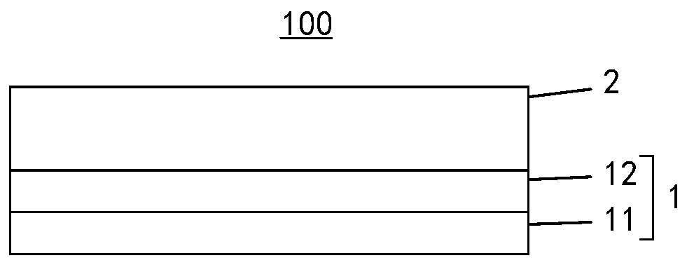
[0033] see figure 1 , this embodiment provides an epitaxial structure 100 , including a composite base electrode layer 1 and an emitter layer 2 fabricated based on the composite base electrode layer 1 .

[0034] Wherein, the composite base electrode layer 1 is a double-layer material structure, including a first base electrode layer 11 and a second base electrode layer 12 made on the basis of the first base electrode layer 11 . The material of the first base electrode layer 11 includes GaAs, and the material of the second base electrode layer 12 includes In x Ga 1-x As. In x Ga 1-x Compared with GaAs, As is a material with a lower energy gap. When used in transistors, it can improve the effect of conduction band spiking, reduce the turn-on voltage of transistors, and reduce power consumption.

[0035] In the second base electrode layer 12, in the direction close to the emitter layer 2, the In content is equal, that is, figure 1 The In content of the second base electrode...

no. 2 example

[0051] This embodiment provides an epitaxial structure 100 , which differs from the epitaxial structure 100 provided in the first embodiment in that the composition of In in the second base electrode layer 12 is different.

[0052] The epitaxial structure 100 includes a composite base electrode layer 1 and an emitter layer 2 . The composite base electrode layer 1 is a double-layer material structure, including a first base electrode layer 11 and a second base electrode layer 12 made on the basis of the first base electrode layer 11 . Wherein, the first base electrode layer 11 and the emitter layer 2 are the same as those in the first embodiment, and will not be repeated here.

[0053] In in the second base electrode layer 12 x Ga 1-x As, in the direction close to the emitter layer 2, the value of x gradually increases. That is to say, figure 1 In the second base electrode layer 12, the In content gradually increases as the thickness increases, and the increasing speed can ...

no. 3 example

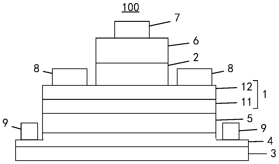
[0059] This embodiment provides an epitaxial structure 100 , which is further designed as an epitaxial structure 100 suitable for HBT (Heterojunction Bipolar Transistor) on the basis of the epitaxial structure 100 provided in the first embodiment or the second embodiment.

[0060] see image 3 , the epitaxial structure 100 includes a substrate 3 , a sub-collector layer 4 , a collector layer 5 , a composite base electrode layer 1 , an emitter layer 2 and a cap layer 6 grown sequentially from bottom to top. Wherein, the composite base electrode layer 1 and the emitter layer 2 adopt the structure in the first embodiment or the second embodiment.

[0061] In addition, an emitter metal contact layer 7 is disposed above the emitter layer 2, and the emitter metal contact layer 7 covers the cap layer 6 and is in ohmic contact with the emitter layer 2, wherein the cap layer 6 is etched with a A via through which the emitter metal contact layer 7 passes. A base electrode metal contact...


PUM

PropertyMeasurementUnit
Thicknessaaaaaaaaaa

Abstract

The invention provides an epitaxial structure and a low-conduction voltage transistor and relates to the technical field of semiconductors and communication. The low on-voltage transistor includes anepitaxial structure. The epitaxial structure includes a composite base electrode layer and an emitter layer. The composite base electrode layer comprises a first base electrode layer and a second baseelectrode layer manufactured based on the first base electrode layer. The material of the first base electrode layer comprises GaAs, and the material of the second base electrode layer comprises InxGa1-xAs. The composite base electrode layer can reduce an energy gap of the base electrode layer so that the conductive band peak effect between the base electrode layer and the emitter layer is reduced, when the composite base electrode layer is applied to the transistor, the on-voltage can be reduced, and the power consumption is reduced. An ohmic contact layer is more easily formed on the secondbase electrode layer by adopting Pt, the thickness of Pt can be reduced, the quantity of Pt driven into the composite base electrode layer is reduced, so that the situation that a device generates interface composite current is reduced, and the reliability test of the device is more stable and reliable.

Description

technical field [0001] The present application relates to the field of semiconductor and communication technologies, and in particular, relates to an epitaxial structure and a low turn-on voltage transistor. Background technique [0002] In power amplifiers currently used in 3G or 4G, power added efficiency (referred to as "PAE") is a very important parameter. PAE is defined as the ratio of the difference between the output power Pout and the input power Pin to the DC input power Pdc, namely: (Pout-Pin) / Pdc. PAE is a pointer indicating the quality of PA efficiency, and the larger the value, the more power loss of the power amplifier can be suppressed. To improve the DC power consumption, the first step is to reduce the conduction voltage (Von), the knee voltage ("Vk" for short) and the offset voltage ("Voff" for short). However, the turn-on voltage of the transistor used in the existing power amplifier is too large, and it is difficult to reduce, resulting in high power co...

Claims


Application Information

Patent Timeline
IPC IPC(8): H01L29/737H01L29/10H01L29/205
CPCH01L29/7371H01L29/1004H01L29/205
Inventor 林科闯颜志泓魏鸿基
Owner XIAMEN SANAN INTEGRATED CIRCUIT
Why Eureka
Try Eureka