
Wafer surface flatness detection method and incomplete exposure unit flatness detection compensation method

A technology of surface flatness and exposure unit, which is applied in the direction of measuring devices, optical devices, instruments, etc., can solve the problems of wrong flatness information, inaccurate flatness, and the Y value cannot be obtained by the exposure unit, so as to ensure the quality of graphics , reduce the effect of defocus

Active Publication Date: 2019-12-31
SHANGHAI HUALI INTEGRATED CIRCUTE MFG CO LTD
View PDF12 Cites 3 Cited by
  • Summary
  • Abstract
  • Description
  • Claims
  • Application Information

AI Technical Summary

Problems solved by technology

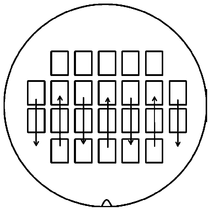
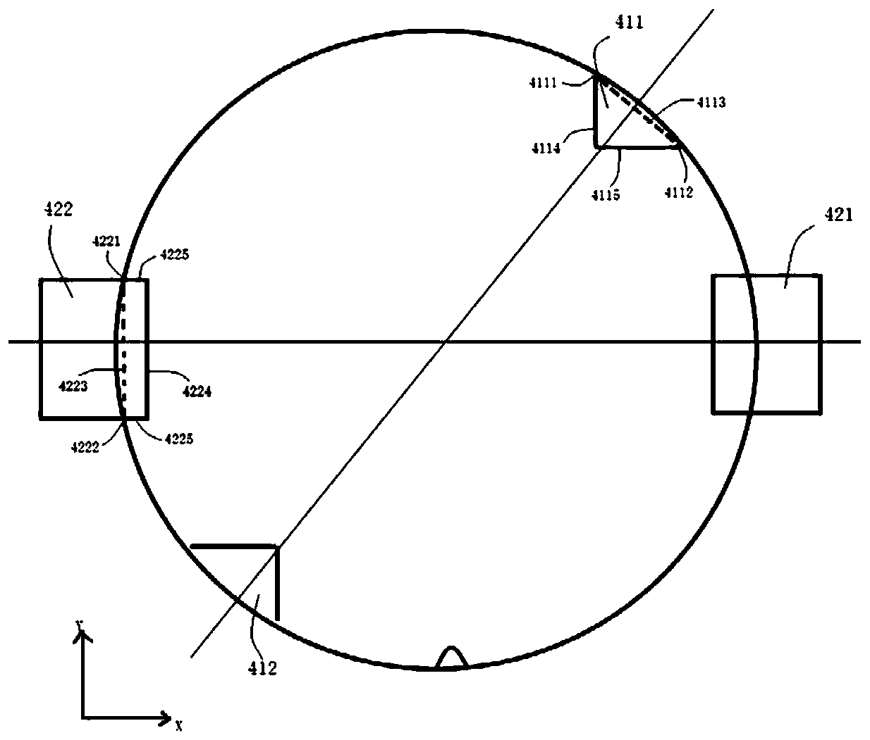
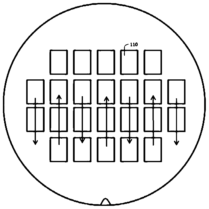
Under this requirement, an incomplete exposure unit with a small crystal edge cannot obtain an accurate Y value, because an exposure unit with a small area may not be able to satisfy two complete detection sensor scans at the same time.
The lack of Y value will cause inaccurate flatness in the exposure unit, resulting in wrong flatness information during exposure, and in serious cases, it will cause defocus

Method used


Image

  • Wafer surface flatness detection method and incomplete exposure unit flatness detection compensation method
  • Wafer surface flatness detection method and incomplete exposure unit flatness detection compensation method
  • Wafer surface flatness detection method and incomplete exposure unit flatness detection compensation method

Examples


Embodiment Construction

[0036] The technical solutions in the present invention will be clearly and completely described below in conjunction with the accompanying drawings. Apparently, the described embodiments are part of the embodiments of the present invention, not all of them. Based on the embodiments of the present invention, all other embodiments obtained by persons of ordinary skill in the art without making creative efforts belong to the protection scope of the present invention.

[0037] In an embodiment of the present invention, a method for detecting the flatness of a wafer surface is provided. The method for detecting the flatness of a wafer surface in an embodiment of the present invention includes: S1: providing a wafer, and exposing the wafer according to an exposure program To form a plurality of exposure units; S2: Determine the complete exposure unit and the incomplete exposure unit on the wafer, and calculate the number B of detection sensors in the incomplete exposure unit, the ca...


PUM


Abstract

The invention relates to a wafer surface flatness detection method and an incomplete exposure unit flatness detection compensation method, and relates to a semiconductor integrated circuit manufacturing technology. S-shaped scanning is still adopted for flatness detection for a complete exposure unit and an incomplete exposure unit with the number of detection sensors being greater than or equal to 2 within the range on the surface of a wafer. For an incomplete exposure unit with the number of detection sensors being less than 2 within the range at the edge, rotation is conducted so as to enable the scanning direction of a photoetching machine to be approximately perpendicular to a connecting line between two points at which the incomplete exposure unit on the wafer is tangent to the waferedge, thereby enabling more than one detection sensor to fall into the incomplete exposure unit to compensate the exposure unit of the photoetching machine, acquiring accurate flatness information inthe whole wafer surface, reducing the occurrence of defocusing, and ensuring the pattern quality after exposure in the whole wafer.

Description

technical field [0001] The invention relates to semiconductor integrated circuit manufacturing technology, in particular to a wafer surface flatness detection and an incomplete exposure unit flatness detection and compensation method. Background technique [0002] In the semiconductor integrated circuit manufacturing technology, with the continuous improvement of the integration of semiconductor integrated circuits and the development of semiconductor technology, the size of semiconductor devices is continuously reduced, and the key dimensions are becoming smaller and smaller, which brings higher The requirements and challenges of lithography, the process window of lithography is also greatly reduced. In order to obtain accurate patterns, it is necessary to ensure that lithography exposure is performed at the best focal length, so as to minimize the probability of defocus. [0003] In the existing exposure process, before the wafer is exposed, the topography of the wafer sur...

Claims


Application Information

Patent Timeline
Patent Type & Authority Applications(China)
IPC IPC(8): G01B11/30
CPCG01B11/30
Inventor 王建涛
Owner SHANGHAI HUALI INTEGRATED CIRCUTE MFG CO LTD
Learn More