Electronic skin having classified voltage crest structure and preparation method of electronic skin

A technology of electronic skin and conductivity, which is applied in the field of sensors, can solve problems such as limited application prospects and low sensitivity, and achieve the effects of good repeatability, high sensitivity, and fast response recovery ability

Active Publication Date: 2020-01-17
HUAZHONG UNIV OF SCI & TECH
View PDF15 Cites 4 Cited by
  • Summary
  • Abstract
  • Description
  • Claims
  • Application Information

AI Technical Summary

Problems solved by technology

However, low sensitivity and irregular surface morphology of sandpaper templates limit their application prospects

Method used


Image

  • Electronic skin having classified voltage crest structure and preparation method of electronic skin
  • Electronic skin having classified voltage crest structure and preparation method of electronic skin
  • Electronic skin having classified voltage crest structure and preparation method of electronic skin

Examples


preparation example Construction

[0054] The present invention also provides a method for preparing an electronic skin with a hierarchical pressure peak structure, which includes the following steps:

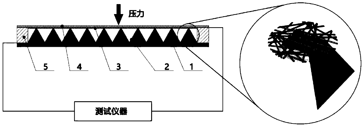
[0055] S1 prepares a flexible substrate sputtered with a pressure sensitive layer on the surface:

[0056] First prepare a master template with a raised structure on the surface, wash and dry, then use the master template to prepare an inverted mold and prepare an isolation layer on the surface of the inverted mold, and then use the inverted mold with an isolation layer on the surface to prepare a flexible substrate, and finally Sputter a pressure sensitive layer on the surface of the substrate to obtain a flexible substrate with a pressure sensitive layer sputtered on the surface, specifically:

[0057] S11 master template production: the metal block is made into a master template with an array of raised structures on the surface through a CNC grinder;

[0058] Pre-treatment of the S12 master template: The master templ...

Embodiment 1

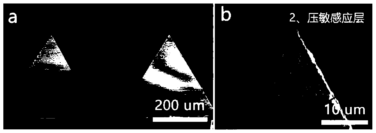
[0081] This embodiment is the preparation of an electronic skin with a hierarchical pressure peak structure based on magnetron sputtering gold, PVP nanowire nets, and a micro-pyramid array. The specific preparation is carried out by the following steps:

[0082] 1) The metal block is made into a master template with a pyramid array on the surface through a CNC grinder;

[0083] 2) After sonicating the finished master template with ethanol for 10 minutes, sonicating with deionized water for 10 minutes, then sonicating with ethanol for 10 minutes, drying at 50°C;

[0084] 3) Pour the pre-mixed polydimethylsiloxane (PDMS) on the surface of the master template, after drying, peel off to obtain the first inverted mold;

[0085] 4) Sputtering a gold layer on the surface of the first inverted mold;

[0086] 5) Pour the premixed polydimethylsiloxane (PDMS) on the surface of the first inverted mold, and after drying, peel off to obtain a flexible substrate with a micro-pyramid array, the micro-p...

Embodiment 2

[0094] This implementation is the preparation of an electronic skin with a hierarchical pressure peak structure based on graphene, PVP nanowire nets and micro-hemisphere arrays, and the specific preparation is carried out by the following steps:

[0095] 1) Using photolithography to prepare a master template with micro-hemispherical pits on a silicon wafer;

[0096] 2) After sonicating the finished master template with ethanol for 30 minutes, sonicating with deionized water for 15 minutes, then sonicating with ethanol for 20 minutes, drying at 40°C;

[0097] 3) Pour the pre-mixed polydimethylsiloxane (PDMS) on the surface of the master template, after drying, peel off to obtain the first inverted mold;

[0098] 4) Layered self-assembled graphene on the surface of the first inverted mold to form an isolation layer;

[0099] 5) Pour the premixed polydimethylsiloxane (PDMS) on the surface of the first inverted mold, and after drying, peel off to obtain a flexible substrate with a micro-hem...


PUM

PropertyMeasurementUnit
electrical conductivityaaaaaaaaaa
thicknessaaaaaaaaaa
diameteraaaaaaaaaa

Abstract

The invention belongs to the technical field of sensors, and discloses electronic skin having a classified voltage crest structure and a preparation method of the electronic skin. The electronic skincomprises a flexible substrate and an electronic encapsulating layer, wherein a protrusion structure is formed in the surface of the flexible substrate, a pressure sensitive induction layer is splashed to the surface of the protrusion structure, the electrode encapsulating layer lies in that a flexible film having electric conduction function is arranged on the lower surface, a reticular insulation net layer is prepared on the lower surface, the electronic encapsulating layer is arranged at the top of the protrusion structure, and the upper insulation net layer is jointed to the top of the protrusion structure; and a holding frame is also arranged between the insulation net layer and the edge of the flexible substrate, the upper surface of the holding frame is bonded with the insulation net layer, and the lower surface is bonded with the flexible substrate. The method comprises the following steps of preparing the flexible substrate to which the surface the pressure sensitive inductionlayer and the flexible substrate are sputtered; preparing the electronic encapsulating layer with the insulation net layer; and preparing the holding frame and performing encapsulating. The electronic skin being high in sensitivity and broad in induction range can be obtained, and has the advantages of being simple and easy to obtain, excellent in properties and the like.

Description

Technical field [0001] The invention belongs to the technical field of sensors, and more specifically, relates to an electronic skin with a hierarchical pressure peak structure and a preparation method thereof. Background technique [0002] The basic principle of a flexible pressure sensor is to convert mechanical pressure excitation into a readable electrical signal. It has received widespread attention because of its potential applications in wearable medical monitoring equipment, soft robots, human-computer interaction, and electronic skin. For example, voice recognition is performed by analyzing the vibration signal of the vocal cords during vocalization, and the heart function is diagnosed by the vibration signal of the heart. [0003] In order for the flexible pressure sensor to perceive various pressure stimuli, the flexible pressure sensor must exhibit excellent performance on two key parameters: one is the detection range (stretchability), and the other is sensitivity. St...

Claims


Application Information

Patent Timeline
Patent Type & Authority Applications(China)
IPC IPC(8): A61B5/0205A61B5/103G01L1/18
CPCA61B5/0205A61B5/021A61B5/08A61B5/1038G01L1/18
Inventor 黄禹吴从义荣佑民张田
Owner HUAZHONG UNIV OF SCI & TECH
Why Eureka
Try Eureka