Storage and transport device for semiconductor wafers and method of use thereof

A transportation device, semiconductor technology, applied in transportation and packaging, containers to prevent mechanical damage, containers, etc., can solve the problems of inconvenient storage of semiconductor wafers, easy pick and place operations, and wear of wafer surfaces.

Active Publication Date: 2021-09-14
杭州翔毅科技有限公司
View PDF5 Cites 0 Cited by
  • Summary
  • Abstract
  • Description
  • Claims
  • Application Information

AI Technical Summary

Problems solved by technology

[0003] The object of the present invention is to provide a storage and transportation device for semiconductor wafers, so as to solve the problems in the prior art that semiconductor wafers are inconvenient to store, and the pick-and-place operation is easy to cause wear on the wafer surface

Method used


Image

  • Storage and transport device for semiconductor wafers and method of use thereof
  • Storage and transport device for semiconductor wafers and method of use thereof
  • Storage and transport device for semiconductor wafers and method of use thereof

Examples


Embodiment Construction

[0036] The following will clearly and completely describe the technical solutions in the embodiments of the present invention with reference to the accompanying drawings in the embodiments of the present invention. Obviously, the described embodiments are only some, not all, embodiments of the present invention. Based on the embodiments of the present invention, all other embodiments obtained by persons of ordinary skill in the art without making creative efforts belong to the protection scope of the present invention.

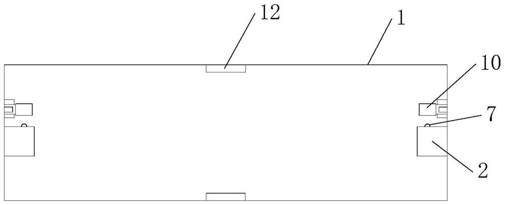
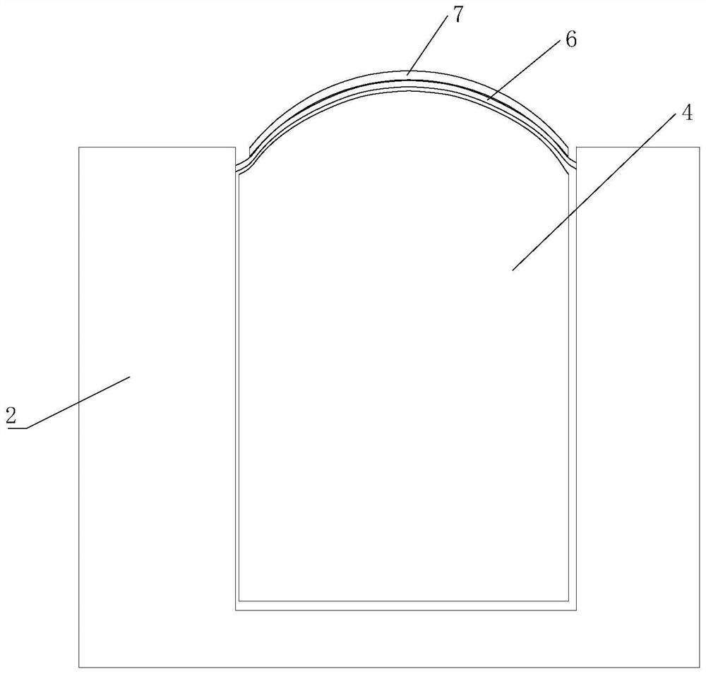
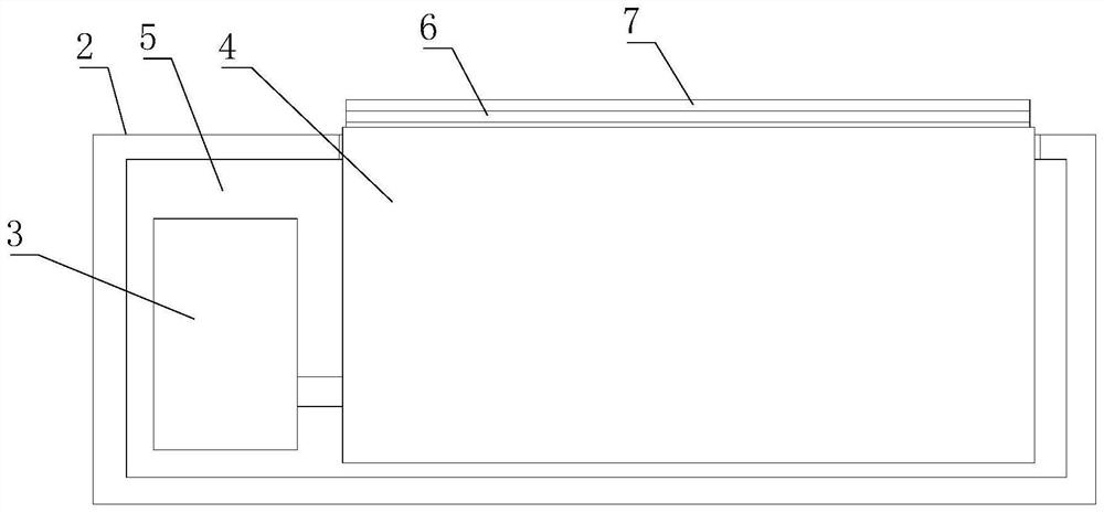
[0037] see Figures 1 to 6 , the present invention provides a technical solution: a storage and transportation device for semiconductor wafers, including a frame body 1, a storage mechanism for placing semiconductor wafers, a dust suction mechanism for cleaning the surface of the storage mechanism, and a control The control device for the operation of the storage mechanism and the dust suction mechanism. The storage mechanism includes two symmetrically arrange...


PUM


Abstract

The invention relates to the technical field of semiconductor production equipment, in particular to a storage and transportation device for semiconductor wafers, which includes a rack body, a storage mechanism for placing semiconductor wafers, a dust suction mechanism for cleaning the surface of the storage mechanism, and a A control device for controlling the operation of the storage mechanism and the dust suction mechanism. The storage mechanism includes two symmetrically arranged storage racks and a lifting mechanism installed on the storage racks. The dust suction mechanism is provided with two, two Two dust-absorbing mechanisms are arranged corresponding to corresponding skins respectively, and the dust-absorbing mechanisms include push cylinders, sliders, brush bodies and electromagnetic valves. The present invention can be used to place semiconductor wafers, and can avoid semiconductor wafers from being worn out.

Description

technical field [0001] The invention relates to the technical field of semiconductor production equipment, and the specific field is a storage and transportation device for semiconductor wafers and a use method thereof. Background technique [0002] During the processing and production of semiconductor wafers, they are stored, transferred and transported by transfer devices. However, most of the current semiconductor wafer racks are single-layer, so that each rack can only place one semiconductor substrate, resulting in low substrate conveying efficiency on the conveyor belt. Moreover, most of the racks are open. In the field of semiconductors, it is necessary to ensure the purity of the substrate surface to avoid particle contamination of the substrate by attaching tiny particles to the substrate. This makes the open rack easy to increase the particle size of the substrate surface during the transfer of the substrate. In addition, in the process of picking and placing the w...

Claims


Application Information

Patent Timeline
Patent Type & Authority Patents(China)
IPC IPC(8): B65D81/05
CPCB65D81/05
Inventor 王华珍
Owner 杭州翔毅科技有限公司
Why Eureka
Try Eureka