

Three-dimensional memory and forming method thereof
A memory and three-dimensional technology, applied in the semiconductor field, can solve the problems affecting the electrical connection of the word line contact hole etching process, affecting the performance of the memory, and the residue of conductive materials, so as to improve the collapse phenomenon, prevent metal residue, and strengthen the support effect.
- Summary
- Abstract
- Description
- Claims
- Application Information
AI Technical Summary
Problems solved by technology
Method used
Image

Examples
Embodiment Construction
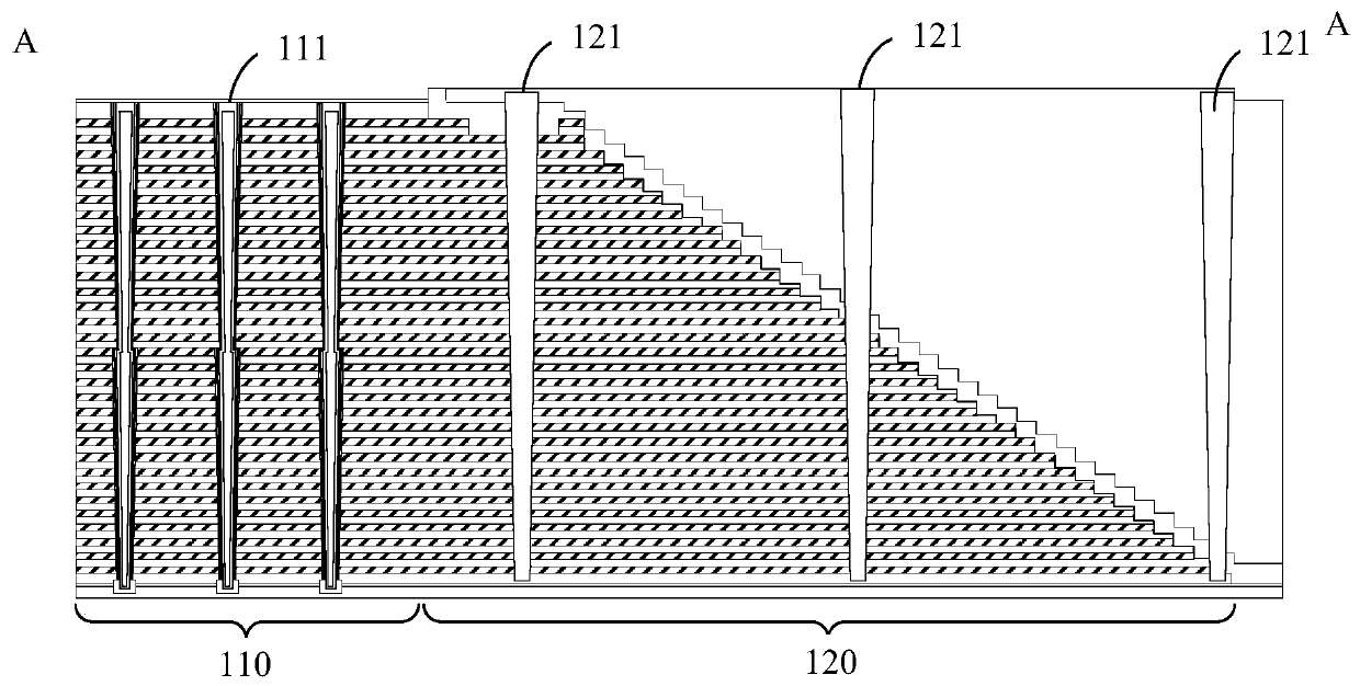
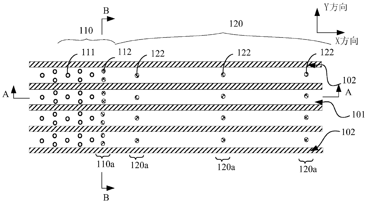
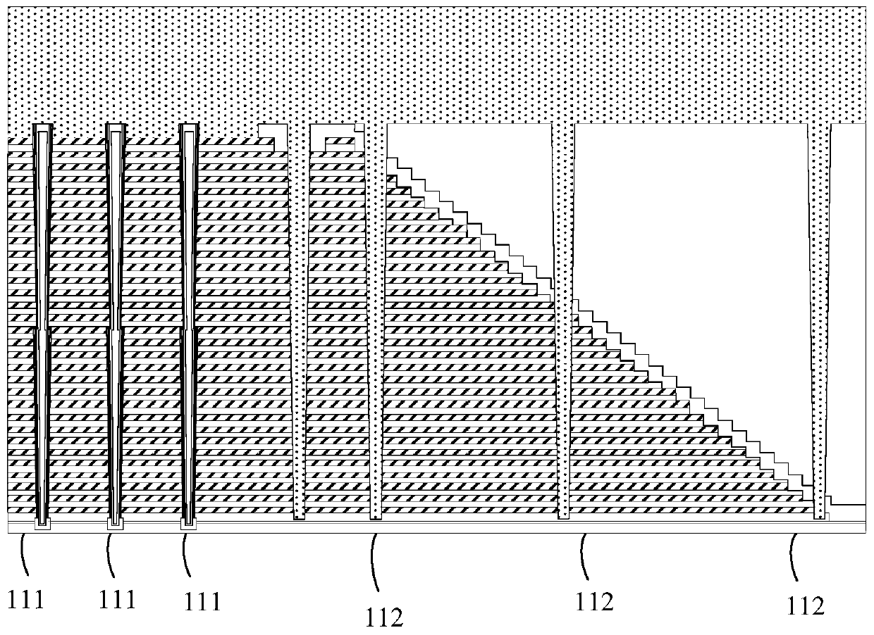
[0032] In order to make the above objectives, features and advantages of the present invention more obvious and understandable, the specific embodiments of the present invention will be described in detail below with reference to the accompanying drawings.
[0033] In the following description, many specific details are set forth in order to fully understand the present invention, but the present invention can also be implemented in other ways different from those described herein, so the present invention is not limited by the specific embodiments disclosed below.
[0034] As shown in the present application and claims, unless the context clearly indicates exceptions, the words "a", "an", "an" and / or "the" do not specifically refer to the singular, but may also include the plural. Generally speaking, the terms "including" and "including" only suggest that the clearly identified steps and elements are included, and these steps and elements do not constitute an exclusive list, and th...
PUM
| Property | Measurement | Unit |
|---|---|---|
| thickness | aaaaa | aaaaa |
| size | aaaaa | aaaaa |
| thickness | aaaaa | aaaaa |
Abstract
Description
Claims
Application Information