
Formation method of metal gate and semiconductor device

A technology of metal gates and semiconductors, applied in semiconductor devices, semiconductor/solid-state device manufacturing, electrical components, etc., can solve problems such as metal gates are prone to defects, reduce the control ability of metal gates, and achieve the effect of avoiding holes

Active Publication Date: 2020-01-24
SEMICON MFG INT (SHANGHAI) CORP +1
View PDF15 Cites 0 Cited by
  • Summary
  • Abstract
  • Description
  • Claims
  • Application Information

AI Technical Summary

Problems solved by technology

[0003] After the gate size is reduced, when filling metal materials into smaller grooves to form a metal gate, defects are prone to appear inside the metal gate, which reduces the control ability of the metal gate

Method used


Image

  • Formation method of metal gate and semiconductor device
  • Formation method of metal gate and semiconductor device
  • Formation method of metal gate and semiconductor device

Examples


no. 1 example

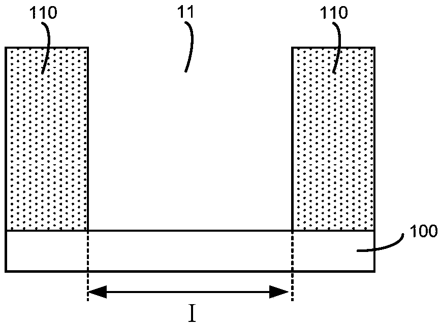
[0038] Please refer to figure 1 , an interlayer dielectric layer 110 is formed on the semiconductor substrate 100 , and a first groove 11 is formed in the interlayer dielectric layer 110 .

[0039] The semiconductor substrate 100 serves as a basis for semiconductor device processes. The material of the semiconductor substrate 100 is polysilicon. In an embodiment of the present invention, the semiconductor substrate 100 includes other semiconductor components (not shown).

[0040] The interlayer dielectric layer 110 plays an insulating role for isolating different structures in the device. In the embodiment of the present invention, the interlayer dielectric layer 110 is formed above the semiconductor substrate 100, and the material of the interlayer dielectric layer 110 is SiO 2 .

[0041] A first groove 11 is formed in the interlayer dielectric layer 110 for subsequent formation of a metal gate therein. figure 1 The area I in the center represents the area range of the...

no. 2 example

[0084] Compared with the first embodiment, the second embodiment of the present invention differs in that, in the method for forming the metal gate in the second embodiment, after forming the first groove and before forming the dummy gate, it also includes The groove sidewall forms a sidewall, and the second groove is formed above the sidewall. The formation method and positional relationship of the structures of other parts are consistent with the first embodiment.

[0085] Please refer to Figure 6 A side wall 211 is formed on the side wall of the first groove, and a second groove 22 is formed above the side wall 211 .

[0086] The formation method and positional relationship of the semiconductor substrate 200 , the interlayer dielectric layer 210 , the first groove, and the dummy gate 220 are consistent with those of the first embodiment, and will not be repeated here.

[0087] Forming the spacer wall 211 can further optimize the function of isolating subsequent metal gat...

no. 3 example

[0102] The difference between the metal gate forming method of the third embodiment of the present invention and the second embodiment is that the second groove is formed by etching part of the interlayer dielectric layer and the spacer. The formation processes of other structures are consistent with the second embodiment.

[0103] Please refer to Figure 8 , forming second grooves 32 on both sides of the dummy gate 320 .

[0104] The process conditions for forming the second groove 32 , and finally the position and size range of the second groove 32 are consistent with those of the second embodiment, and will not be repeated here.

[0105] Obviously, in the embodiment of the present invention, the second groove 32 is formed by etching the sidewall 311 and part of the interlayer dielectric layer 310 adjacent to the sidewall 311, so the bottom of the second groove 32 includes the sidewall 311 The top and part of the interlayer dielectric layer. The process conditions for for...


PUM

PropertyMeasurementUnit
sizeaaaaaaaaaa

Abstract

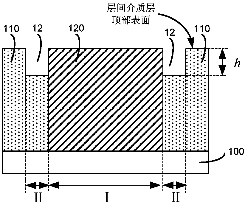
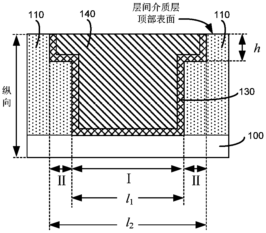
The invention discloses a formation method of a metal gate. The formation method comprises the following steps that: a semiconductor substrate and an interlayer dielectric layer are provided, whereinthe interlayer dielectric layer is formed on the semiconductor substrate; a first groove is formed in the interlayer dielectric layer; a pseudo gate filling the first groove is formed; etching is performed to form second grooves, wherein the second grooves are formed in two sides of the upper part of the pseudo gate, and one side wall of each second groove comprises a part of a pseudo gate side wall; the pseudo gate is removed, a third groove is formed, wherein the third groove comprises the first groove and the second groove; and a high-k dielectric layer covering the inner surface of the third groove is formed, the third groove is filled with a metal material, so that a metal gate can be formed, wherein the metal gate comprises the high-k dielectric layer and the metal material. With theformation method of the metal gate of the invention adopted, defects such as holes and dislocation in the metal gate can be effectively avoided.

Description

technical field [0001] The invention relates to the field of semiconductor manufacturing, in particular to a method for forming a metal gate and a semiconductor device. Background technique [0002] With the continuous reduction of the size of semiconductor components, the traditional polysilicon gate can no longer meet the requirements of use. The emergence of the metal gate (Metal Gate) makes semiconductor devices develop in a more refined direction. Subsequently, the use of high-k dielectric layers further optimized the control role of metal gates and improved the performance of semiconductor devices. [0003] After the size of the gate is reduced, when the smaller groove is filled with metal material to form the metal gate, defects are likely to appear inside the metal gate, which reduces the control ability of the metal gate. [0004] Therefore, there is an urgent need for a method for forming a metal gate that avoids defects inside the metal gate. Contents of the i...

Claims


Application Information

Patent Timeline
Patent Type & Authority Applications(China)
IPC IPC(8): H01L21/28H01L21/336H01L29/423
CPCH01L21/28114H01L21/28079H01L29/66545H01L29/42376
Inventor 韩秋华涂武涛徐柯
Owner SEMICON MFG INT (SHANGHAI) CORP
Learn More