Low turn-on voltage gan microwave diode based on low work function anode metal and preparation method

A technology of turn-on voltage and low work function, applied in the field of microelectronics, can solve the problems of large turn-on voltage of microwave diodes, large metal work function difference, and high Schottky barrier, and achieves reduced turn-on voltage, small work function difference, The effect of reducing the contact barrier

Active Publication Date: 2020-11-10
XIDIAN UNIV
View PDF5 Cites 0 Cited by
  • Summary
  • Abstract
  • Description
  • Claims
  • Application Information

AI Technical Summary

Problems solved by technology

But also due to its material properties, when GaN materials are used in microwave diode devices, due to the large difference in metal work function, the Schottky barrier of the device is relatively high, and the turn-on voltage of microwave diodes is larger than that of traditional Si-based and GaAs-based diodes. , which greatly affects the efficiency of
[0004] Traditional microwave diodes based on AlGaN / GaN structure mostly use metals such as Ni and Pt to achieve Schottky contact with the AlGaN layer. Due to the high barrier height, the turn-on voltage of the device is mostly above 1V, making it difficult to operate in low-power rectification, detection, etc. Therefore, making GaN microwave diodes with low turn-on voltage can greatly improve device performance and expand its application fields, which has great practical significance

Method used


Image

  • Low turn-on voltage gan microwave diode based on low work function anode metal and preparation method
  • Low turn-on voltage gan microwave diode based on low work function anode metal and preparation method

Examples


Embodiment 1

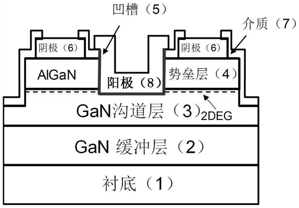
[0041] Example 1, a low turn-on voltage GaN microwave diode with a SiN layer thickness of 200nm, an anode groove etched to 5nm below the AlGaN / GaN interface, and an anode metal of Mo / Au with a thickness of 30 / 200nm was fabricated.

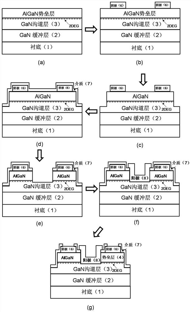
[0042] Step 1, epitaxial wafer cleaning, such as figure 2 (a).

[0043] The epitaxial wafer with AlGaN / GaN structure was soaked in HF acid solution or HCl acid solution for 30s, then placed in acetone solution, absolute ethanol solution and deionized water for 5min ultrasonic cleaning each, and then blown dry with nitrogen.

[0044] Step 2, make GaN microwave diode cathode, such as figure 2 (b).

[0045] 2a) On a clean epitaxial wafer, perform uniform coating, baking, photolithography and development of the cathode area of ​​the device in sequence, and use electron beam evaporation equipment to deposit Ti / Al / Ni / Au metal stacks on the epitaxial wafer with a thickness of 22 / 140 / 55 / 45nm;

[0046] 2b) Soak the epitaxial wafer deposited with Ti / A...

Embodiment 2

[0062] Example 2, making a low turn-on voltage GaN microwave diode with a SiN layer thickness of 300nm, an anode groove etched to 10nm below the AlGaN / GaN interface, and an anode metal of W / Au with a thickness of 40 / 200nm:

[0063] Step 1, epitaxial wafer cleaning, such as figure 2 (a).

[0064] The specific implementation of this step is the same as step 1 of Embodiment 1.

[0065] Step 2, making GaN microwave diode cathode, such as figure 2 (b).

[0066] The specific implementation of this step is the same as that of step 2 in Embodiment 1.

[0067] Step 3, making countertop isolation, such as figure 2 (c).

[0068] The specific implementation of this step is the same as that of step 3 in Embodiment 1.

[0069] Step 4, use plasma-enhanced chemical vapor deposition equipment to deposit a SiN dielectric with a thickness of 300nm on the epitaxial wafer after mesa isolation, such as figure 2 (d).

[0070] Step five, make the anode groove, such as figure 2 (e).

[...

Embodiment 3

[0078] Embodiment 3, making SiO 2 A low turn-on voltage GaN microwave diode with a layer thickness of 200nm, an anode groove etched to 15nm below the AlGaN / GaN interface, and an anode metal of Mo with a thickness of 200nm:

[0079] Step A, epitaxial wafer cleaning, such as figure 2 (a).

[0080] The specific implementation of this step is the same as step 1 of Embodiment 1.

[0081] Step B, making GaN microwave diode cathode, such as figure 2 (b).

[0082] The specific implementation of this step is the same as that of step 2 in Embodiment 1.

[0083] Step C, making countertop isolation, such as figure 2 (c).

[0084] The specific implementation of this step is the same as that of step 3 in Embodiment 1.

[0085] Step D, depositing SiN dielectric. Such as figure 2 (d).

[0086] Deposit SiO with a thickness of 200nm on the mesa-isolated epitaxial wafer using plasma-enhanced chemical vapor deposition equipment 2 medium.

[0087] Step E, make the anode groove, suc...


PUM

PropertyMeasurementUnit
thicknessaaaaaaaaaa
thicknessaaaaaaaaaa
thicknessaaaaaaaaaa

Abstract

The invention discloses a low-turn-on-voltage GaN microwave diode based on low-work-function anode metal and a preparation method thereof, and mainly solves the problem of high turn-on voltage of theGaN microwave diode. The device is performed on an AlGaN / GaN epitaxial wafer. The epitaxial wafer comprises a substrate (1), an epitaxial buffer layer (2), a GaN channel layer (3) and an AlGaN barrierlayer (4) which are arranged from bottom to top. A circular groove (5) is arranged in the channel layer and the barrier layer, and an annular cathode (6) is arranged on the peripheral barrier layer of the groove. A medium (7) is arranged in the region of the AlGaN barrier layer apart from the groove and the cathode. An anode (8) is arranged on the bottom, side walls and edge media of the groove,and the anode is laminated with low work function metal Mo or W and metal Au. The turn-on voltage of the GaN microwave diode can be significantly reduced and the device performance can be improved andthe diode can be widely applied to microwave rectification and microwave limiting.

Description

technical field [0001] The invention belongs to the technical field of microelectronics, in particular to a GaN microwave diode with low turn-on voltage, which can be used for microwave rectification or microwave amplitude limiting. [0002] technical background [0003] As a wide-bandgap semiconductor material, GaN material has great advantages in electrical properties. Because of its strong spontaneous polarization and piezoelectric polarization effects, the AlGaN / GaN heterojunction structure will induce High-concentration two-dimensional electron gas, because the electrons are confined in the potential well, and the impurity doping in this region is very small, so the ionized impurity scattering and alloy disorder scattering are small, the two-dimensional electron gas has extremely high mobility and electron Saturation rate, and due to the inherent wide bandgap properties of GaN materials, its critical breakdown field strength is extremely large, which is suitable for maki...

Claims


Application Information

Patent Timeline
Patent Type & Authority Patents(China)
IPC IPC(8): H01L29/88H01L29/417H01L21/329
CPCH01L29/417H01L29/66219H01L29/882
Inventor 张进成党魁周弘张涛张苇杭宁静郝跃
Owner XIDIAN UNIV
Why Eureka
Try Eureka