Display device, display substrate thereof, and manufacturing method of display substrate

A technology for display substrates and display areas, applied in semiconductor devices, electrical components, circuits, etc., can solve problems such as affecting the overall consistency of the screen, and achieve the effects of reliable performance, no detachment and delamination, and good bonding effect.

Active Publication Date: 2020-12-04
KUNSHAN GO VISIONOX OPTO ELECTRONICS CO LTD
View PDF4 Cites 0 Cited by
  • Summary
  • Abstract
  • Description
  • Claims
  • Application Information

AI Technical Summary

Problems solved by technology

[0002] With the rapid development of display devices, users have higher and higher requirements for screen-to-body ratio. Since cameras, sensors, earpieces and other components need to be installed above the screen, a part of the area above the screen is usually reserved in the prior art for the installation of the above-mentioned Components, such as the front notch area of ​​the iPhone X, affect the overall consistency of the screen, and the full-screen display has attracted more and more attention from the industry

Method used


Image

  • Display device, display substrate thereof, and manufacturing method of display substrate
  • Display device, display substrate thereof, and manufacturing method of display substrate
  • Display device, display substrate thereof, and manufacturing method of display substrate

Examples


Embodiment Construction

[0089] In order to make the above objects, features and advantages of the present invention more comprehensible, specific embodiments of the present invention will be described in detail below in conjunction with the accompanying drawings.

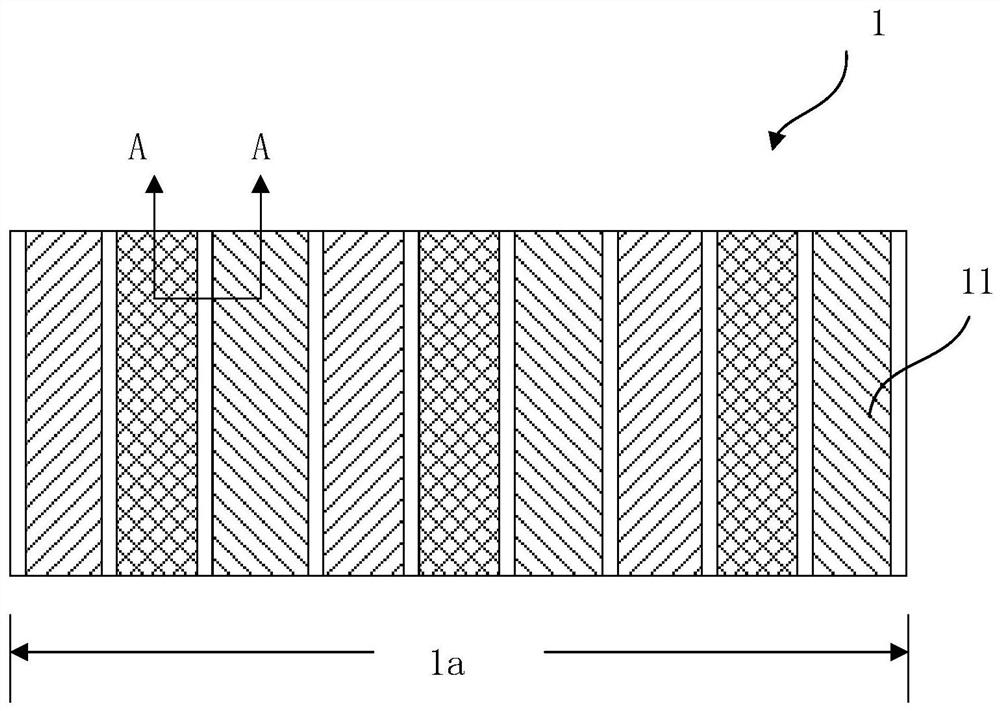
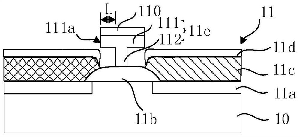
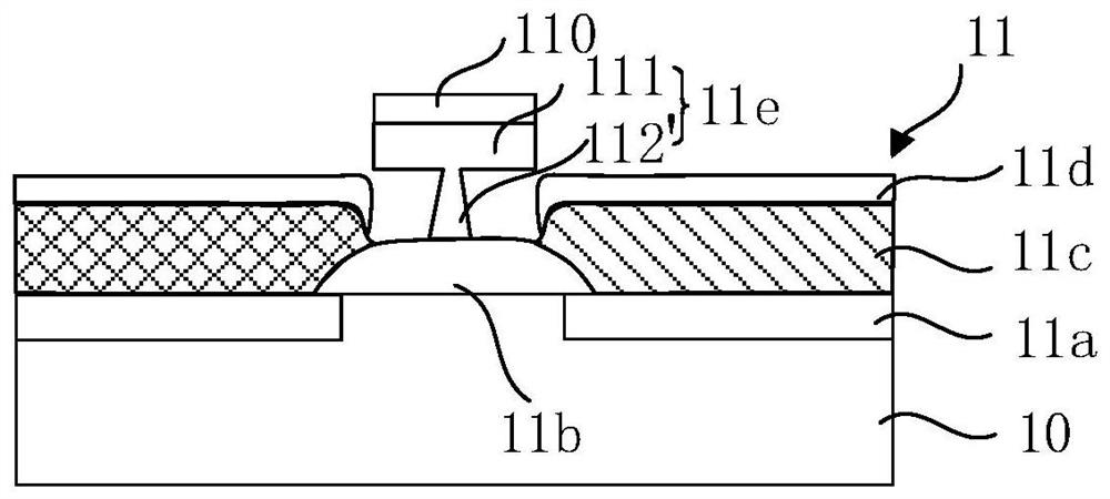
[0090] figure 1 It is a top view of the display panel in an embodiment of the present invention; Fig. 2(a) is along figure 1 2( b ) and FIG. 2( c ) are schematic diagrams of two deformation structures of the first sub-pixel in FIG. 2( a ).

[0091] refer to figure 1 As shown in FIG. 2(c), the display substrate 1 includes a transparent display area 1a, and the transparent display area 1a includes: a light-transmitting substrate 10 and a plurality of first sub-pixels 11 located on the light-transmitting substrate 10; each first sub-pixel The pixel 11 includes a first electrode 11a, a first pixel definition layer 11b on the first electrode 11a, a first light-emitting material layer 11c in the opening of the first pixel definition layer 11b,...


PUM

PropertyMeasurementUnit
heightaaaaaaaaaa

Abstract

The invention provides a display device, a display substrate thereof, and a manufacturing method of the display substrate. The display substrate includes a light-transmitting substrate and a plurality of first sub-pixels; each first sub-pixel includes a first electrode, a first pixel definition layer, a first sub-pixel A first luminescent material layer and a second electrode in the opening of the pixel definition layer; the first pixel definition layer has isolation columns for separating the second electrodes of the adjacent first sub-pixels; the isolation columns are T-shaped, T-shaped The isolation column is an integral molding structure. Because the partition part is long, the T-shaped isolation column has a good automatic partition effect on the vapor-deposited conductive material layer; the T-shaped isolation column is integrally formed and has a single-layer structure. The partition part and the support part have the same material, and the pattern is realized in the same process Therefore, the bonding effect between the partition part and the support part is good, there is no delamination phenomenon, and the performance is reliable.

Description

technical field [0001] The present invention relates to the technical field of display devices, in particular to a display device, a display substrate, and a method for manufacturing the display substrate. Background technique [0002] With the rapid development of display devices, users have higher and higher requirements for screen-to-body ratio. Since cameras, sensors, earpieces and other components need to be installed above the screen, a part of the area above the screen is usually reserved in the prior art for the installation of the above-mentioned Components, such as the front notch area of ​​the iPhone X, affect the overall consistency of the screen, and the full-screen display has attracted more and more attention from the industry. Contents of the invention [0003] The object of the present invention is to provide a display device for a full screen, a display substrate, and a manufacturing method of the display substrate. [0004] In order to achieve the above...

Claims


Application Information

Patent Timeline
Patent Type & Authority Patents(China)
IPC IPC(8): H01L27/32
CPCH10K59/00H10K59/121H10K59/122H10K59/12H10K50/822H10K50/828H10K59/60H10K59/353H10K71/00H10K59/1201
Inventor 梁超吴昊迟帅杰唐静楼均辉陶国胜范俊
Owner KUNSHAN GO VISIONOX OPTO ELECTRONICS CO LTD
Why Eureka
Try Eureka