Display device and manufacturing method thereof

A technology for a display device and a manufacturing method, which is applied to electrical components, electric solid-state devices, circuits, etc., and can solve problems such as light leakage and display quality degradation of a display device

Active Publication Date: 2020-02-11
AU OPTRONICS CORP
View PDF9 Cites 2 Cited by
  • Summary
  • Abstract
  • Description
  • Claims
  • Application Information

AI Technical Summary

Problems solved by technology

However, in such a structure, some components may cause light leakage in the display device due to reflection of ambient light, resulting in a decrease in display quality

Method used


Image

  • Display device and manufacturing method thereof
  • Display device and manufacturing method thereof
  • Display device and manufacturing method thereof

Examples


Embodiment Construction

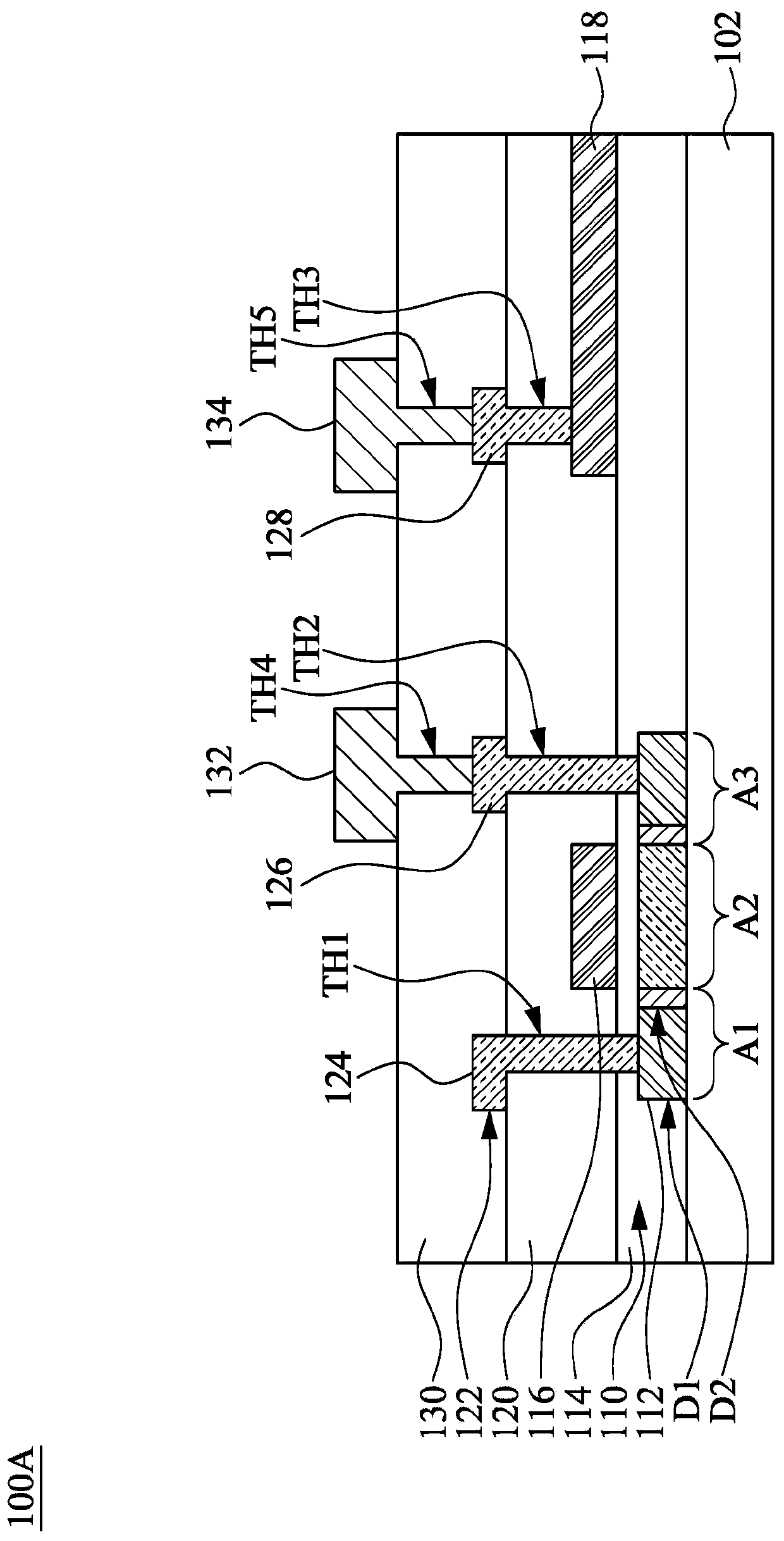
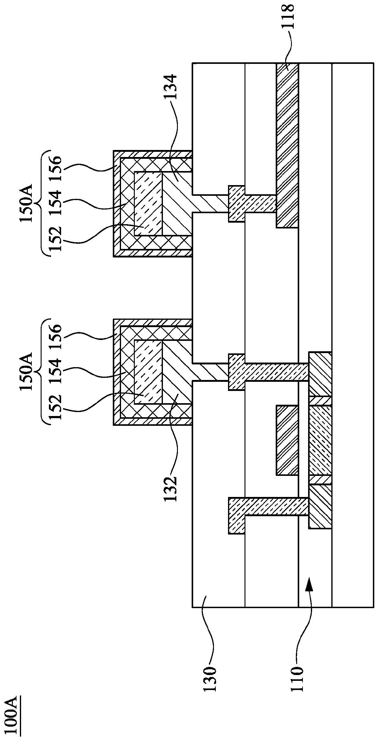
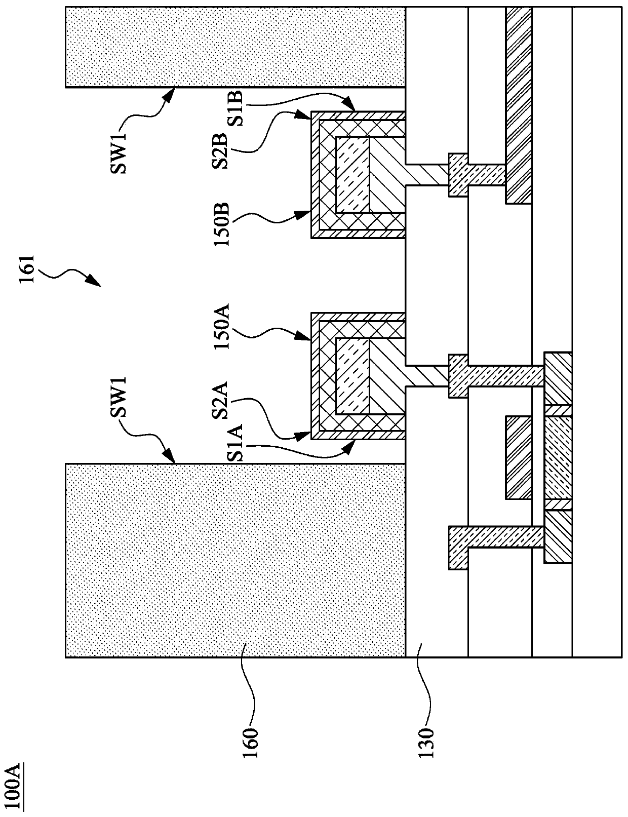
[0076] A number of implementations of the present disclosure will be disclosed below with the accompanying drawings. For the sake of clarity, many practical details will be described together in the following description. However, it should be understood that these practical details should not be used to limit the present disclosure. That is, in some embodiments of the present disclosure, these practical details are unnecessary. In addition, for the sake of simplifying the drawings, some conventional structures and elements will be shown in a simple schematic way or omitted in the drawings.

[0077] Herein, it is understandable that terms such as first, second and third are used to describe various elements or regions. These terms can be used to identify a single element or region. Therefore, a first element or region hereinafter may also be referred to as a second element or region without departing from the spirit of the present disclosure. As used herein, "about" or "sub...


PUM

PropertyMeasurementUnit
thicknessaaaaaaaaaa
thicknessaaaaaaaaaa
thicknessaaaaaaaaaa

Abstract

The present disclosure relates to a display device and a manufacturing method thereof. The manufacturing method of the display device includes the following steps: forming a bonding pad over a dielectric layer. A light-shielding material is formed over the dielectric layer. The temperature of the light-shielding material is raised to cure the light-shielding material into a light-shielding layer.During the process of curing the light-shielding material into the light-shielding layer, the light-shielding material flows to a part of the surface contacting the bonding pad. A light emitting element is electrically connected to the bonding pad.

Description

technical field [0001] The disclosure relates to a display device and a manufacturing method thereof. Background technique [0002] In recent years, light-emitting diodes (light-emitting diodes; LEDs) have been widely used in consumer electronics applications. Light-emitting diodes have many advantages, such as lower energy consumption, longer lifetime, smaller size and faster switching, so they are suitable for use as light sources. In addition, light emitting diodes have also begun to be introduced into display devices. Light emitting diodes in display devices can be driven by thin film transistors or circuit layers. However, in such a structure, part of the elements may cause light leakage in the display device due to reflection of ambient light, resulting in a decrease in display quality. Therefore, how to improve the above problems has become one of the current research and development topics in related fields. Contents of the invention [0003] An embodiment of t...

Claims


Application Information

Patent Timeline
Patent Type & Authority Applications(China)
IPC IPC(8): H01L33/44H01L33/62H01L27/15
CPCH01L27/153H01L33/44H01L33/62H01L2933/0025H01L2933/0066H01L25/0753H01L25/167H01L27/124H01L33/58H01L27/1214H01L2933/0058
Inventor 阮丞禾曾建洲侯智元
Owner AU OPTRONICS CORP
Why Eureka
Try Eureka