Free ground film, circuit board and preparation method of free ground film

A circuit board and printed circuit board technology, applied in the electronic field, can solve problems such as inability to interfere with charge derivation, connection failure between free grounding film and electromagnetic shielding film, and influence on signal transmission of circuit boards

Pending Publication Date: 2020-02-11
GUANGZHOU FANGBANG ELECTRONICS
View PDF0 Cites 2 Cited by
  • Summary
  • Abstract
  • Description
  • Claims
  • Application Information

AI Technical Summary

Problems solved by technology

However, in the process of implementing the present invention, the inventors found that there are at least the following problems in the prior art: at high temperature, due to the expansion of the conductive adhesive layer, the conductive particles in the conductive adhesive layer that were originally in contact with each other will be pulled apart or the conductive particles that were originally in contact with each other will be separated. The conductive particles in contact with the electromagnetic shielding film are pulled apart, resulting in the failure of the connection between the free grounding film and the electromagnetic shielding film, so that the interference charges accumulated on the electromagnetic shielding film cannot be effectively exported, and then form a source of interference, affecting the signal transmission of the circuit board

Method used


Image

  • Free ground film, circuit board and preparation method of free ground film
  • Free ground film, circuit board and preparation method of free ground film
  • Free ground film, circuit board and preparation method of free ground film

Examples


Embodiment 1

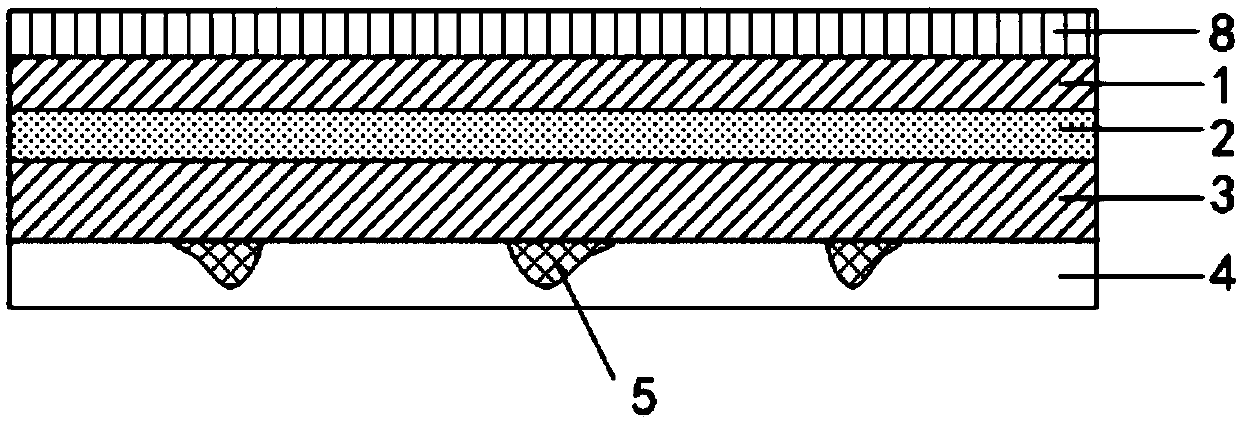
[0066] See figure 1 , the embodiment of the present invention provides a free grounding film, which includes a first conductor layer 1, a conductive adhesive layer 2, a second conductor layer 3 and an adhesive film layer 4 which are sequentially stacked; the second conductor layer 3 is close to the Conductive protrusions 5 are provided on one side of the adhesive film layer 4;

[0067] see Figure 9 , when the free grounding film is used for the grounding of the printed circuit board, an electromagnetic shielding film 9 is provided on the printed circuit board 11, and the electromagnetic shielding film 9 includes a shielding layer 91 and an insulating layer 90 stacked. The free grounding film is pressed together with the electromagnetic shielding film 9 through the adhesive film layer 4, and the conductive protrusion 5 pierces through the adhesive film layer 4 and the insulating layer 90 and is electrically connected with the shielding layer 91 . Wherein, the material of th...

Embodiment 2

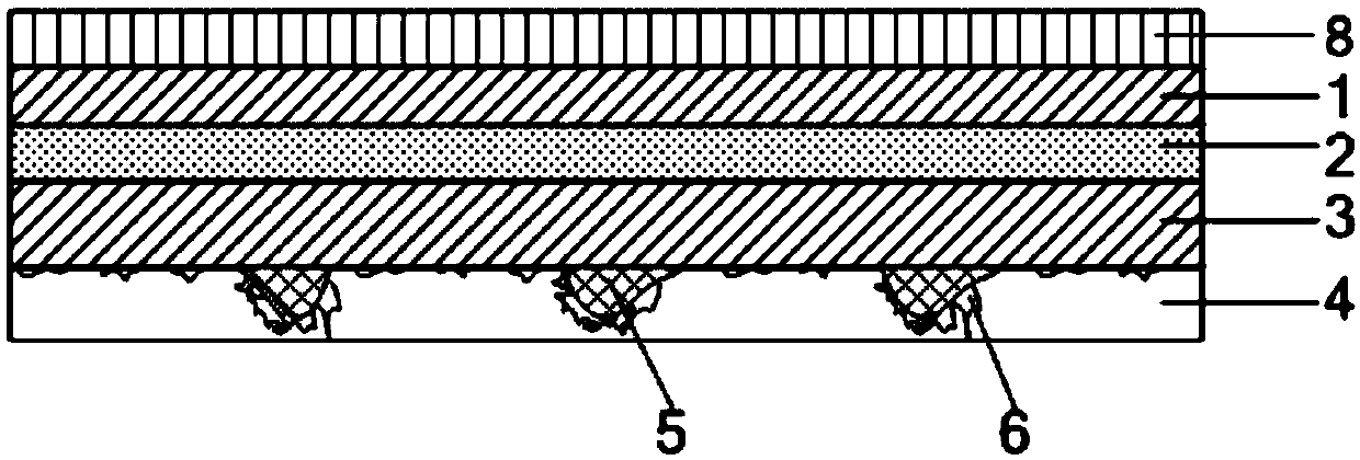
[0104] see Figure 4, the embodiment of the present invention provides another free grounding film, which includes a first conductor layer 1, a conductive adhesive layer 2, a second conductor layer 3, a third conductor layer 7 and an adhesive film layer 4; the first conductor layer 1. The conductive adhesive layer 2 and the second conductive layer 3 are sequentially stacked; the second conductive layer 3 is provided with conductive protrusions 5 on the side away from the conductive adhesive layer 2; the third The conductor layer 7 is covered on the one side of the second conductor layer 3, and the position of the third conductor layer 7 covering the conductive protrusion 5 forms a raised portion 70 (the raised portion 70 and the The relationship between the conductive bumps 5 can be one-to-one correspondence, one-to-many correspondence, or many-to-one correspondence, etc. When the relationship between the raised portion 70 and the conductive bumps 5 is a one-to-one corresponde...

Embodiment 3

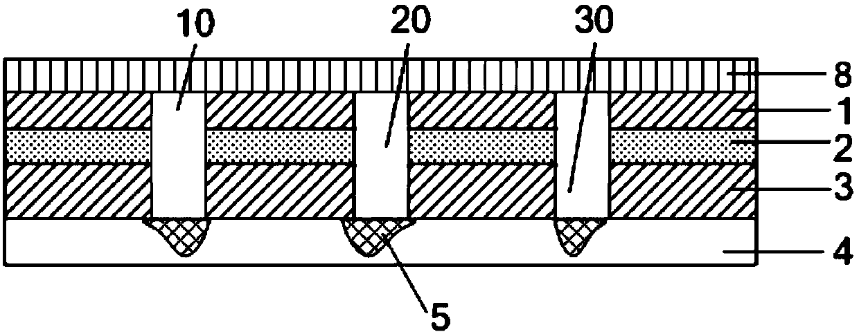
[0120] see Figure 9 and Figure 10 , the embodiment of the present invention provides a circuit board, including a printed circuit board 11 and an electromagnetic shielding film 9 provided on the printed circuit board 11 .

[0121] see Figure 9 , the circuit board also includes the free grounding film of any solution in the first embodiment; the electromagnetic shielding film 9 includes a shielding layer 91 and an insulating layer 90 stacked, and the free grounding film passes through the adhesive film The layer 4 is pressed against the electromagnetic shielding film 9 , and the conductive protrusion 5 pierces through the adhesive film layer 4 and the insulating layer 90 and is electrically connected to the shielding layer 91 .

[0122] or, see Figure 10 , the circuit board also includes the free grounding film of any solution in the second embodiment; the electromagnetic shielding film 9 includes a shielding layer 91 and an insulating layer 90 stacked, and the free grou...


PUM

PropertyMeasurementUnit
Heightaaaaaaaaaa
Thicknessaaaaaaaaaa
Thicknessaaaaaaaaaa

Abstract

The embodiment of the invention provides a free ground film, a circuit board and a preparation method of the free ground film. The free ground film includes a first conductor layer, a conductive adhesive layer, a second conductor layer, and an adhesive film layer, which are sequentially stacked. The second conductor layer is provided with a conductive protrusion on the side near the adhesive filmlayer. When the free ground film is used for grounding of a printed circuit board, an electromagnetic shielding film is arranged on the printed circuit board. The free ground film and the electromagnetic shielding film are pressed together through the adhesive film layer. The conductive protrusion penetrates the adhesive film layer and the insulation layer of the electromagnetic shielding film andis electrically connected with the shielding layer of the electromagnetic shielding film. Interference charges accumulated on the shielding layer are effectively led out. An interference source formed by the accumulation of the interference charges is avoided, and thus the integrity of signal transmission is effectively ensured.

Description

technical field [0001] The invention relates to the field of electronics, in particular to a free grounding film, a circuit board and a method for preparing the free grounding film. Background technique [0002] With the rapid development of the electronics industry, electronic products are further developed toward miniaturization, light weight, and high-density assembly, which greatly promotes the development of flexible circuit boards, thereby realizing the integration of component devices and wire connections. Flexible circuit boards can be widely used in industries such as mobile phones, liquid crystal displays, communications and aerospace. [0003] Driven by the international market, functional flexible circuit boards dominate the flexible circuit board market, and an important indicator for evaluating the performance of functional flexible circuit boards is Electromagnetic Interference Shielding (EMI Shielding). With the integration of functions of communication equi...

Claims


Application Information

Patent Timeline
IPC IPC(8): H05K1/02
CPCH05K1/0218H05K2201/0715
Inventor 苏陟高强朱开辉蒋卫平朱海萍
Owner GUANGZHOU FANGBANG ELECTRONICS
Why Eureka
Try Eureka