Inductance component with down-lead electrode and processing method thereof

A processing method and component technology, which is applied to transformer/inductor parts, transformer/inductor coils/windings/connections, electrical components, etc., can solve the problem of reducing the accumulation of printed circuit boards and the overall size of components cannot be effectively reduced , Climbing glue and other issues, to achieve the effect of miniaturization development, good welding effect, and reduced molding size

Pending Publication Date: 2020-02-18
RALEC TECH KUNSHAN LTD
View PDF1 Cites 2 Cited by
  • Summary
  • Abstract
  • Description
  • Claims
  • Application Information

AI Technical Summary

Problems solved by technology

[0003] However, since the terminal electrodes of the existing integrally formed micro-inductors are located on the left and right sides of the component, such as Chinese patent CN201921231975.6, not only the overall size of the component cannot be ef

Method used


Image

  • Inductance component with down-lead electrode and processing method thereof
  • Inductance component with down-lead electrode and processing method thereof
  • Inductance component with down-lead electrode and processing method thereof

Examples


Embodiment Construction

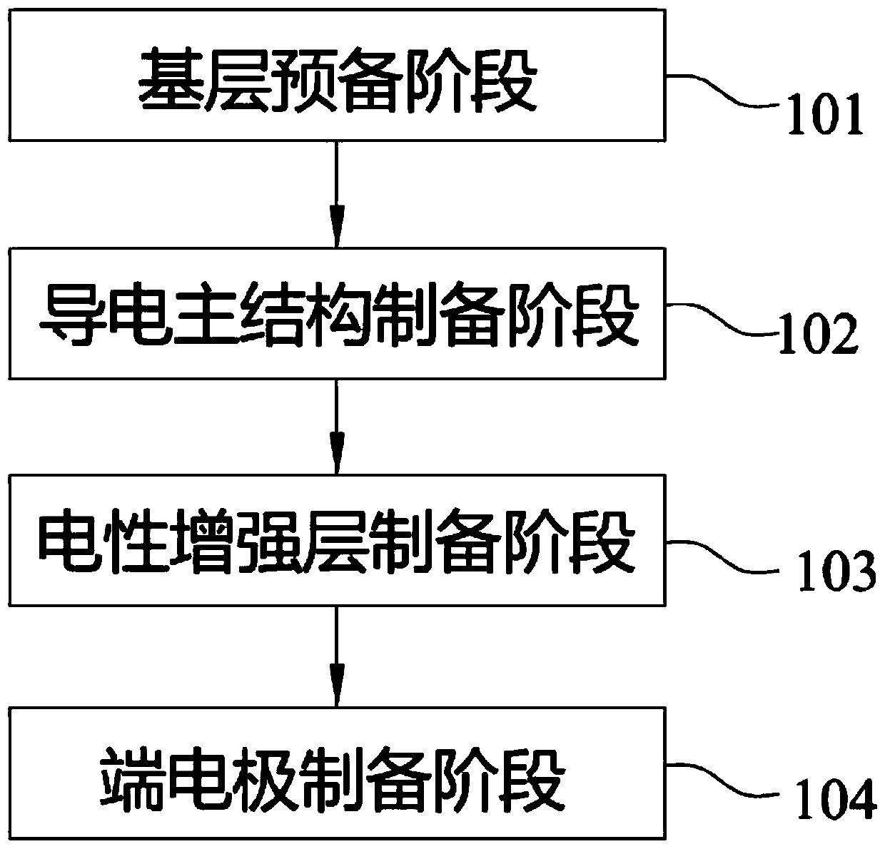
[0015] The implementation of the present invention will be illustrated by specific specific examples below, and those skilled in the art can easily understand other advantages and effects of the present invention from the contents disclosed in this specification.

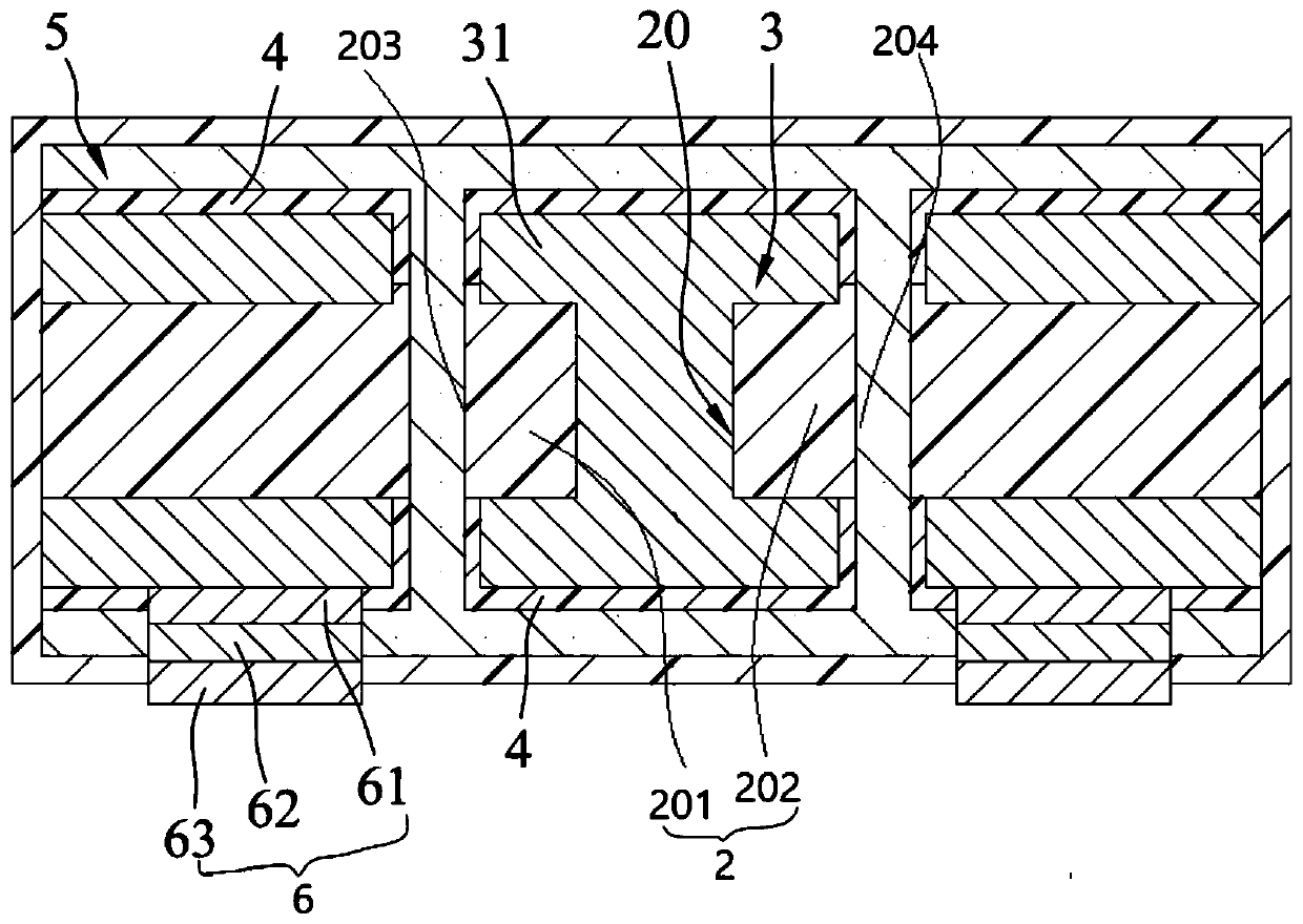
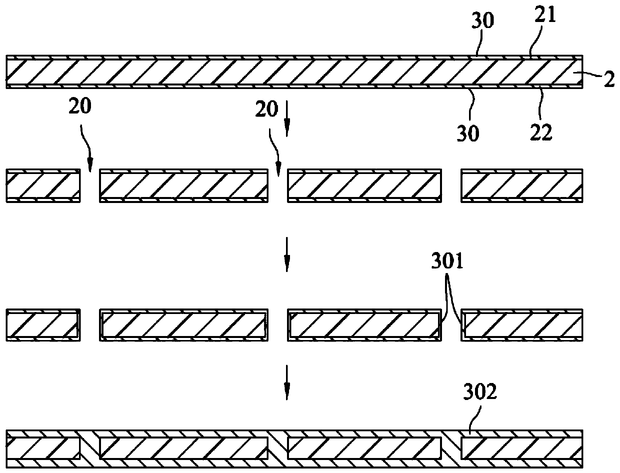
[0016] see figure 1 to Fig. It should be noted that the structures, proportions, sizes, etc. shown in the drawings attached to this specification are only used to match the content disclosed in the specification, for those who are familiar with this technology to understand and read, and are not used to limit the implementation of the present invention. Limiting conditions, so there is no technical substantive meaning, any modification of structure, change of proportional relationship or adjustment of size, without affecting the effect and purpose of the present invention, should still fall within the scope of the present invention. The disclosed technical content must be within the scope covered. At the same time...


PUM


Abstract

The invention relates to a method for processing an inductance component, comprising a first step of a base layer preparation phase; a second step of a conductive main structure preparation phase; a third step of an electrical enhancement layer preparation phase; and a fourth step of a terminal electrode preparation phase. In addition, the present invention also discloses an inductance component prepared by using the method, which includes an insulating substrate 1, an insulating substrate 2, an electrical layer, a first insulating layer, an electrical enhancement layer, a second insulating layer, and a terminal electrode. The electrical layer is arranged between the insulating substrate 1 and the insulating substrate 2. The insulating substrate 1 and the insulating substrate 2 include a through hole 1 and a through hole 2, respectively. The electrical layer is disposed on the upper, lower, front and rear sides of the insulating substrate 1 and on the the upper, lower, front and rear sides of the insulating substrate 2. The first insulating layer is disposed on the upper, lower, front and rear sides and the inner wall of the electrical layer. The method for preparing the inductancecomponent effectively reduces the size of the inductance component, and effectively solves the solder tin creeping when the inductance component is soldered.

Description

technical field [0001] The invention relates to an inductance component with a lead-down electrode and a processing method thereof. Background technique [0002] With the advancement of science and technology, the development of electronic products towards thinner and thinner has been driven by the trend. Therefore, components such as resistors, capacitors, and inductors mounted on printed circuit boards of electronic products must also be reduced in size. In the case of integrally formed micro-inductors, the structure is mainly formed by first forming internal circuits through winding, and after packaging and molding, terminal electrodes for external electrical connection are formed on the left and right sides. [0003] However, since the terminal electrodes of the existing integrally formed micro-inductors are located on the left and right sides of the component, such as Chinese patent CN201921231975.6, not only the overall size of the component cannot be effectively reduc...

Claims


Application Information

Patent Timeline
IPC IPC(8): H01F27/29H01F27/28H01F27/32H01F41/04H01F41/10H01F41/12H01L23/64
CPCH01F27/2804H01F27/292H01F27/324H01F41/041H01F41/10H01F41/125H01L23/645
Inventor 汪晓伟刘建赵斌
Owner RALEC TECH KUNSHAN LTD
Why Eureka
Try Eureka