Substrate integrated waveguide filter based on artificial surface plasmon

An artificial surface plasmon and filter technology, applied to waveguide devices, electrical components, circuits, etc., can solve the problem of reducing the upper sideband cut-off frequency of the filter, unfavorable filter miniaturization and integration, and filter out-of-band suppression Reduced force and other issues, to achieve the effect of improved selectivity, good out-of-band suppression ability, and light weight

Pending Publication Date: 2021-06-04
CHENGDU ZHONGZHITIANCHENG TECH CO LTD
View PDF0 Cites 1 Cited by
  • Summary
  • Abstract
  • Description
  • Claims
  • Application Information

AI Technical Summary

Problems solved by technology

[0005] Most of the artificial surface plasmons used in the currently designed artificial surface plasmons and substrate-integrated waveguide hybrid filters adopt a linear or T-shaped or L-shaped metal slot line arrangement structure, which is limited by the working mechanism of the device. , the traditional substrate-integrated waveguide filter based on artificial surface plasmons has a high upper sideband cut-off frequency, and generally works in the X-band (8-12GHz) and Ku-band (12-18GHz). In order to make this device Working in the S or C band, it is nece

Method used


Image

  • Substrate integrated waveguide filter based on artificial surface plasmon
  • Substrate integrated waveguide filter based on artificial surface plasmon
  • Substrate integrated waveguide filter based on artificial surface plasmon

Examples


Example Embodiment

[0030] Example 1

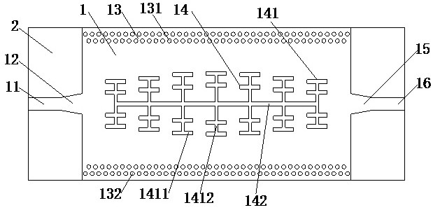
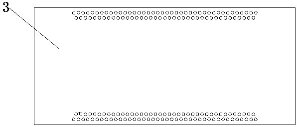
[0031] like figure 1 and figure 2 Shown: a substrate-integrated waveguide filter based on artificial surface plasmons, including a dielectric substrate 2, an upper circuit board 1 located on the upper surface of the dielectric substrate 2 and a lower ground plate 3 located on the lower surface of the dielectric substrate 2, the upper layer The circuit board 1 includes an input port 11 , an ML-SIW transition portion 12 , a substrate integrated waveguide portion 13 , an SIW-ML transition portion 15 and an output port 16 . The English of the microstrip line is Microstrip Line (ML), the English of the substrate integrated waveguide is Substrate integrated waveguide (SIW), the ML-SIW transition part 12 is the microstrip line-substrate integrated waveguide transition part, and the SIW-ML transition part 15 Then it is the substrate integrated waveguide-microstrip line transition part, the input port 11, the output port 16, the ML-SIW transition part, and the SIW...

Example Embodiment

[0036] Example 2

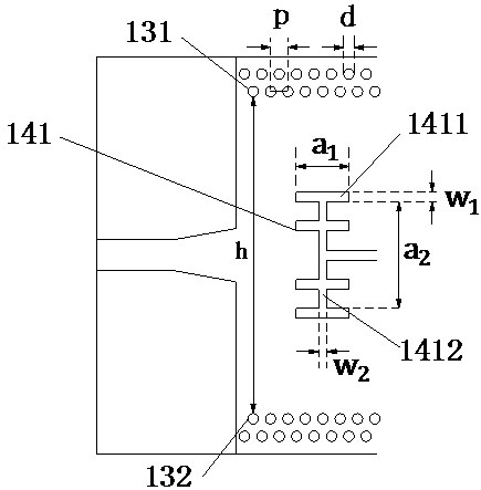
[0037] like figure 1 and image 3 As shown, this embodiment discloses a substrate-integrated waveguide filter based on artificial surface plasmons, and the lower sideband cut-off frequency f of the filter is d It can be adjusted through the metal via hole array structure of the substrate integrated waveguide part 13 . Specifically, the distance between the upper metal via array 131 and the lower metal via array 132 is h, and the lower sideband cut-off frequency of the filter is f d , both satisfy:

[0038]

[0039] In the formula, c is the speed of light in vacuum, and ε is the relative permittivity of the dielectric substrate. From the above formula, it can be obtained that the value of h increases, and the lower sideband cut-off frequency f d Decrease, the h value decreases, then the lower sideband cut-off frequency f d increase. Therefore, adjusting the distance between the upper metal via array 131 and the lower metal via array 132 can change th...

Example Embodiment

[0044] Example 3

[0045] like figure 1 and Figure 4 As shown, this embodiment discloses a substrate-integrated waveguide filter based on artificial surface plasmons, the artificial surface plasmon structure 14 includes N artificial surface plasmon units 141, and the range of N is , 2≤N≤11. As preferred, the value of N is 7, figure 1 The shown filter adopts 7 artificial surface plasmon units 141, and its upper sideband cutoff frequency is as Figure 4 Shown at 7GHz, the lower sideband cutoff frequency is 5GHz, and the filter bandwidth is 2GHz.

[0046] According to the filtering performance requirements of the filter, the artificial surface plasmon structure can be designed as 2 to 11 artificial surface plasmon units. Generally speaking, the higher the operating frequency of the filter, the artificial surface plasmon The less the number of units, at least 2 can be designed. Limited by the working mechanism of the device, the upper sideband cut-off frequency of the tradi...


PUM


Abstract

The invention discloses a substrate integrated waveguide filter based on artificial surface plasmon, and the filter comprises a dielectric substrate, an upper layer circuit board located on the upper surface of the dielectric substrate and a lower layer grounding plate located on the lower surface of the dielectric substrate; the upper layer circuit board comprises an input port, an ML-SIW transition part, a substrate integrated waveguide part, an SIW-ML transition part and an output port; the substrate integrated waveguide part is of an upper-row metal via hole array structure and a lower-row metal via hole array structure which are the same and correspond in parallel; an artificial surface plasmon structure which is formed by metal trough lines and is in bilateral symmetry and up-down symmetry is etched between the upper-row metal via hole array and the lower-row metal via hole array, and the artificial surface plasmon structure comprises N artificial surface plasmon units and a central horizontal trough line. After the cut-off frequency of the upper sideband is reduced, the filter still has a small size, miniaturization and light weight of the filter are facilitated, and good out-of-band rejection capacity is achieved. The upper or lower sideband cut-off frequency of the filter can be adjusted, and the design flexibility is high.

Description

technical field [0001] The invention relates to the technical field of radio frequency communication filtering, in particular to a substrate-integrated waveguide hybrid filter based on artificial surface plasmons. Background technique [0002] In microwave and millimeter wave wireless transceiver systems, the filter is one of the most critical components, which is responsible for frequency band division, spurious wave filtering and frequency selection. The filter based on the substrate integrated waveguide structure has many advantages such as low cost, easy integration, large power capacity and low loss. [0003] Traditional substrate-integrated waveguide filters have two obvious disadvantages. First of all, the out-of-band rejection capability of the substrate integrated waveguide filter is poor, and resonance points often appear near the upper sideband. In order to improve its out-of-band suppression capability, a low-pass filter must be connected in series at the outpu...

Claims


Application Information

Patent Timeline
IPC IPC(8): H01P1/20
CPCH01P1/20
Inventor 贺正军陈鹏杨涛
Owner CHENGDU ZHONGZHITIANCHENG TECH CO LTD
Why Eureka
Try Eureka