Method for manufacturing inductance elements in batches

A technology of inductive components and batch production, which is applied in the field of batch production of inductive components, can solve the problems of low production efficiency and the difficulty of miniaturization of integrally formed micro-inductors in the molding size, and achieve high production efficiency, which is conducive to miniaturization and increases production rate. Effect

Pending Publication Date: 2020-03-24
RALEC TECH KUNSHAN LTD
View PDF0 Cites 3 Cited by
  • Summary
  • Abstract
  • Description
  • Claims
  • Application Information

AI Technical Summary

Problems solved by technology

However, it is difficult to miniaturize the molding size of the integrally formed micro-inductor manufactured in this way, and the overall production efficiency is low.

Method used


Image

  • Method for manufacturing inductance elements in batches
  • Method for manufacturing inductance elements in batches
  • Method for manufacturing inductance elements in batches

Examples


Embodiment Construction

[0031] The implementation of the content of the present invention is illustrated by specific specific examples below, and those skilled in the art can easily understand other advantages and effects of the content of the present invention from the content disclosed in this specification.

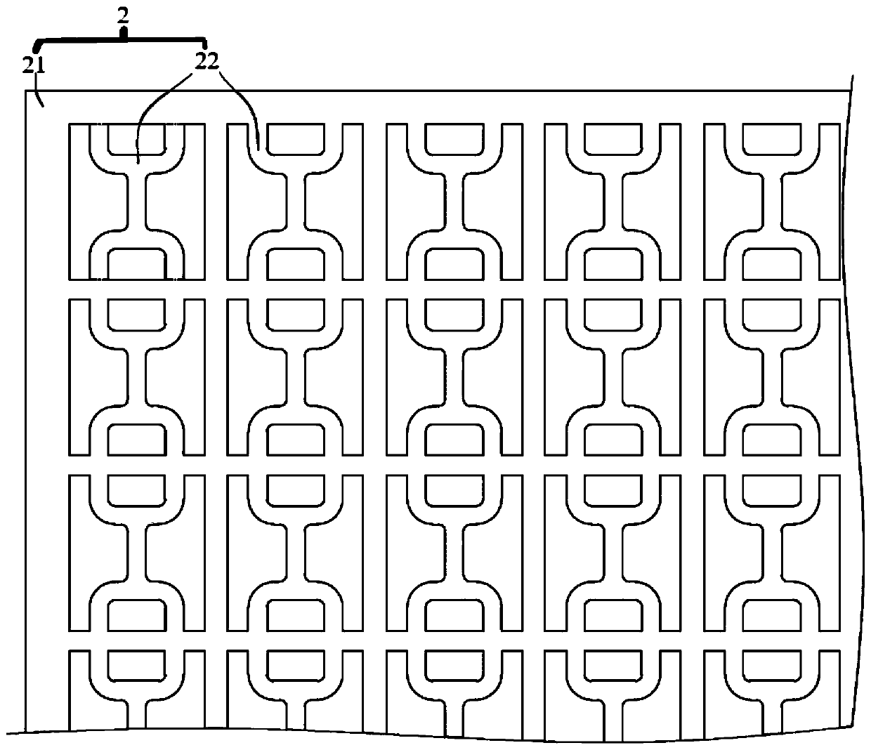
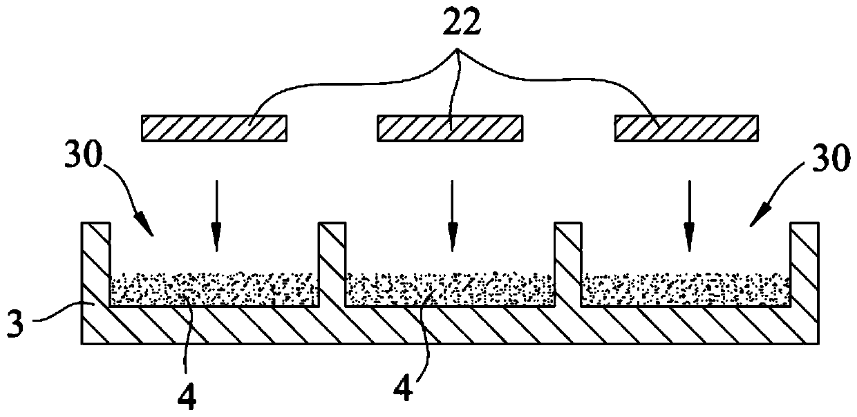
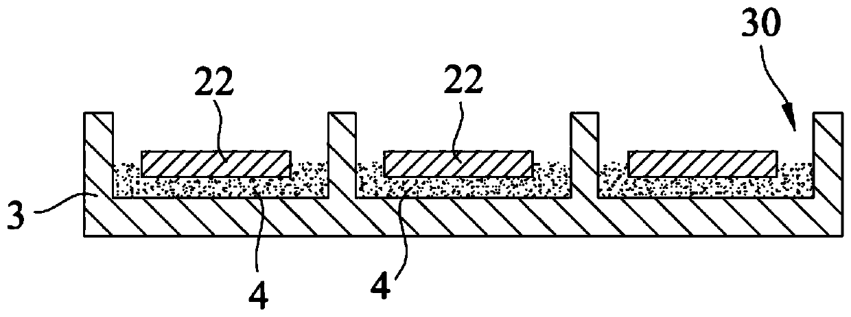
[0032] see Figure 1 to Figure 8 . It should be noted that the structures, proportions, sizes, etc. shown in the drawings attached to this specification are only used to match the content disclosed in the specification, for those who are familiar with this technology to understand and read, and are not used to limit the implementation of the content of the present invention. Therefore, it has no technical substantive meaning. Any modification of structure, change of proportional relationship or adjustment of size shall still fall within the scope of The technical content disclosed in the content of the present invention must be within the scope covered. At the same time, terms such as "uppe...


PUM


Abstract

The invention relates to a method for manufacturing inductance elements in batches. The method comprises the following steps: 1, stamping a conductive substrate to form a main circuit conductor layer;2, arranging a magnetic material with a preset thickness in the first mold, and enabling the plurality of main circuit conductor layers on the conductive substrate to respectively correspond to one mold cavity; 3, punching the main circuit conductor layer on the conductive substrate to enable the main circuit conductor layer to fall onto the magnetic material in the mold cavity in the first mold;4, arranging a magnetic material with a preset thickness on the main line conductor layer in the mold cavity; 5, assembling the second mold and the first mold, pressing the magnetic material, and obtaining a semi-finished product wrapped with the electrical enhancement layer; 6, coating the periphery of the semi-finished product with a coating layer; and 7, in the semi-finished product in the step 6, cutting to remove the coating layer and the electrical enhancement layer at the two ends and part of the lower end of the semi-finished product. The method is simple in manufacturing process, a plurality of inductance elements can be manufactured at a time, and the production efficiency is greatly improved.

Description

technical field [0001] The content of the present invention relates to a method for mass production of inductance elements. Background technique [0002] With the advancement of science and technology, semiconductor technology is becoming more and more sophisticated, and the appearance of various electronic products has gradually developed towards a thinner and shorter shape, and the precision of electronic products is also increasing. The resistors, capacitors or inductors installed in various electronic products The number of such components also increases. Therefore, how to reduce the size of components such as resistors, capacitors, or inductors, and effectively simplify the production process of each component, so as to improve the overall production efficiency has become an important issue. [0003] As far as each component is concerned, taking the integrally formed micro-inductor as an example, the structural process is mainly to form the internal circuit by winding ...

Claims


Application Information

Patent Timeline
Patent Type & Authority Applications(China)
IPC IPC(8): H01F41/00H01F41/02H01F41/04H01F17/04
CPCH01F17/04H01F41/00H01F41/005H01F41/0246H01F41/04H01F2017/048
Inventor 朱华朱翠平卜荣
Owner RALEC TECH KUNSHAN LTD
Why Eureka
Try Eureka