Unlock instant, AI-driven research and patent intelligence for your innovation.

memory device

A memory and main storage technology, applied in static memory, digital memory information, information storage, etc., can solve the problems of difficult size reduction, high production cost, easy to produce defective or damaged storage elements, etc.

Active Publication Date: 2021-09-14
WINBOND ELECTRONICS CORP
View PDF9 Cites 0 Cited by
  • Summary
  • Abstract
  • Description
  • Claims
  • Application Information

AI Technical Summary

Problems solved by technology

[0002] With increasing circuit complexity, the manufacture of various forms of memory devices is inevitably prone to defective or damaged memory elements
One of the common methods to improve the reliability of memory devices is to use error-correcting code memory (ECC memory), however, the memory using ECC technology is accompanied by the problems of difficult reduction in size and high production cost.

Method used


Image

  • memory device
  • memory device
  • memory device

Examples


Embodiment Construction

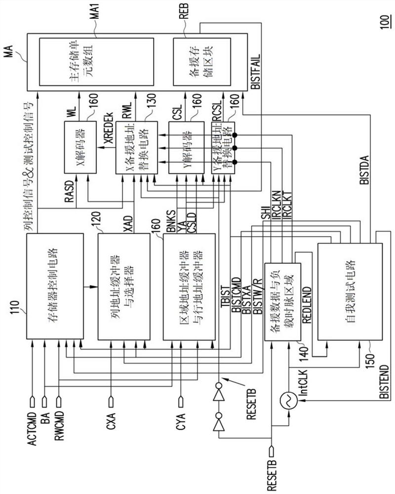
[0067] Please refer to figure 1 , figure 1 A schematic diagram of a memory device according to an embodiment of the present invention is shown. The memory device 100 has a memory cell array MA, a memory control circuit 110, a column address buffer and a selector 120, an X spare address replacement circuit 130, a spare data and load clock area 140, a self-test circuit 150 and a peripheral circuit 160 ( For example, it includes an area address buffer and a row address buffer, an X decoder, a Y decoder, and a Y spare address replacement circuit).

[0068] The storage unit array MA includes the main storage unit array MA1 and the redundant storage block REB. Redundancy memory rows and redundant memory columns are configured in the redundant storage block REB. The row has a spare storage unit, which can replace the bad or damaged storage unit in the main storage unit array MA1 on the circuit, for example, switch the non-volatile storage redundant address (address) through the ele...


PUM


Abstract

The invention provides a memory device, which includes a self-test circuit and a spare address replacement circuit. The self-test circuit is coupled to the main storage unit array, and is used for performing a self-test program on the main storage unit array to provide a self-test signal. The backup address replacement circuit includes a first backup circuit and a second backup circuit. The first backup circuit replaces part of the word line addresses of the main memory cell array with part of the word line addresses of the backup memory block according to the first backup data signal generated by the first test program. The second backup circuit is coupled to the first backup circuit, and replaces the detected error word line addresses in the main memory cell array with another part of the word line addresses of the backup memory block according to the self-test signal.

Description

technical field [0001] The present invention relates to a semiconductor device, in particular to a memory device with self-test function. Background technique [0002] With increasing circuit complexity, various forms of memory devices are inevitably prone to defective or damaged memory elements in the manufacture. One of the common methods to improve the reliability of memory devices is to use error-correcting code memory (ECC memory). However, the memory using ECC technology is accompanied by the problems of difficult reduction in size and high production cost. Contents of the invention [0003] The present invention provides a memory device with a self-test function, which can execute a self-test program after booting and loading backup data of an electronic fuse, and replace bad word line addresses detected in the self-test program, so as to strengthen the memory device reliability. [0004] The spare address replacement circuit of the memory device of the present in...

Claims


Application Information

Patent Timeline
Patent Type & Authority Patents(China)
IPC IPC(8): G11C11/16
CPCG11C11/1677
Inventor 中冈裕司
Owner WINBOND ELECTRONICS CORP