Tunneling field effect transistor and forming method thereof
A tunneling field effect and transistor technology, which is applied in the fields of semiconductor devices, semiconductor/solid-state device manufacturing, electrical components, etc. Shorter time and better performance
- Summary
- Abstract
- Description
- Claims
- Application Information
AI Technical Summary
Problems solved by technology
Method used
Image

Examples
Example Embodiment
[0034] As mentioned in the background art, the performance of tunneling field effect transistors is poor.
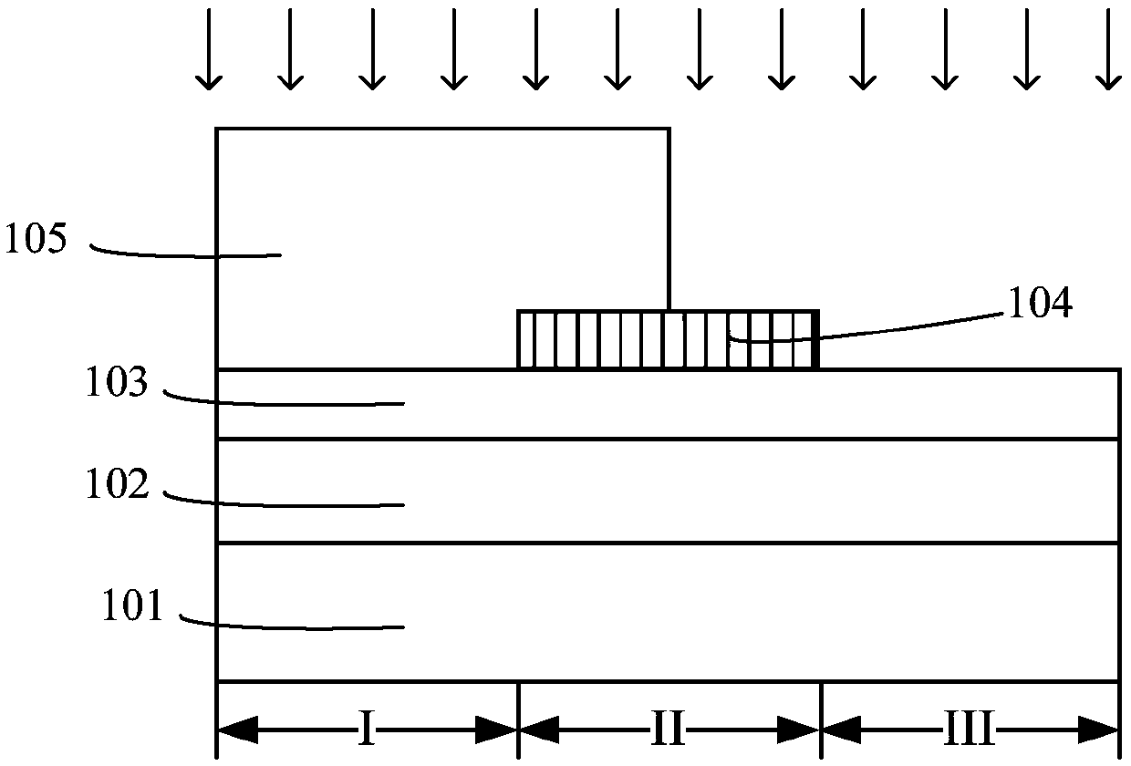
[0035] An embodiment of a method for forming a tunneling field effect transistor includes: providing a substrate, the substrate is silicon-on-insulator, the substrate has a gate structure and sidewalls covering the sidewalls of the gate structure, and the gate The electrode structure covers part of the surface of the substrate; a source region and a drain region are formed in the substrate on both sides of the gate structure, and the drain region is doped with boron ions; the top silicon layer of the source region substrate is removed quickly; Annealing treatment forms a tunnel dielectric layer in the source region, the tunnel dielectric layer covers the sidewall of the substrate under the gate structure; a polysilicon layer is formed in the source region, and arsenic ions are doped in the polysilicon layer.
[0036] However, the material of the source region of the tunneling...
PUM
| Property | Measurement | Unit |
|---|---|---|
| Thickness | aaaaa | aaaaa |
Abstract
Description
Claims
Application Information
 - R&D Engineer
- R&D Manager
- IP Professional
- Industry Leading Data Capabilities
- Powerful AI technology
- Patent DNA Extraction
Browse by: Latest US Patents, China's latest patents, Technical Efficacy Thesaurus, Application Domain, Technology Topic.
© 2024 PatSnap. All rights reserved.Legal|Privacy policy|Modern Slavery Act Transparency Statement|Sitemap