
Electrostatic discharge protection device and operating method of same

An electrostatic discharge protection, electrostatic discharge technology, applied in circuits, electrical components, electrical solid devices, etc., can solve problems such as low holding voltage, power overload, etc.

Active Publication Date: 2020-02-25
MACRONIX INT CO LTD
View PDF4 Cites 0 Cited by
  • Summary
  • Abstract
  • Description
  • Claims
  • Application Information

AI Technical Summary

Problems solved by technology

[0004] However, parasitic SCRs have a significantly lower holding voltage relative to the trigger voltage
Therefore, once the parasitic silicon-controlled rectifier is activated during high-voltage operation, it is easy to have the risk of electrical overstress (Electrical Overstress, EOS) or latch up in subsequent general operations.

Method used


Image

  • Electrostatic discharge protection device and operating method of same
  • Electrostatic discharge protection device and operating method of same
  • Electrostatic discharge protection device and operating method of same

Examples


Embodiment Construction

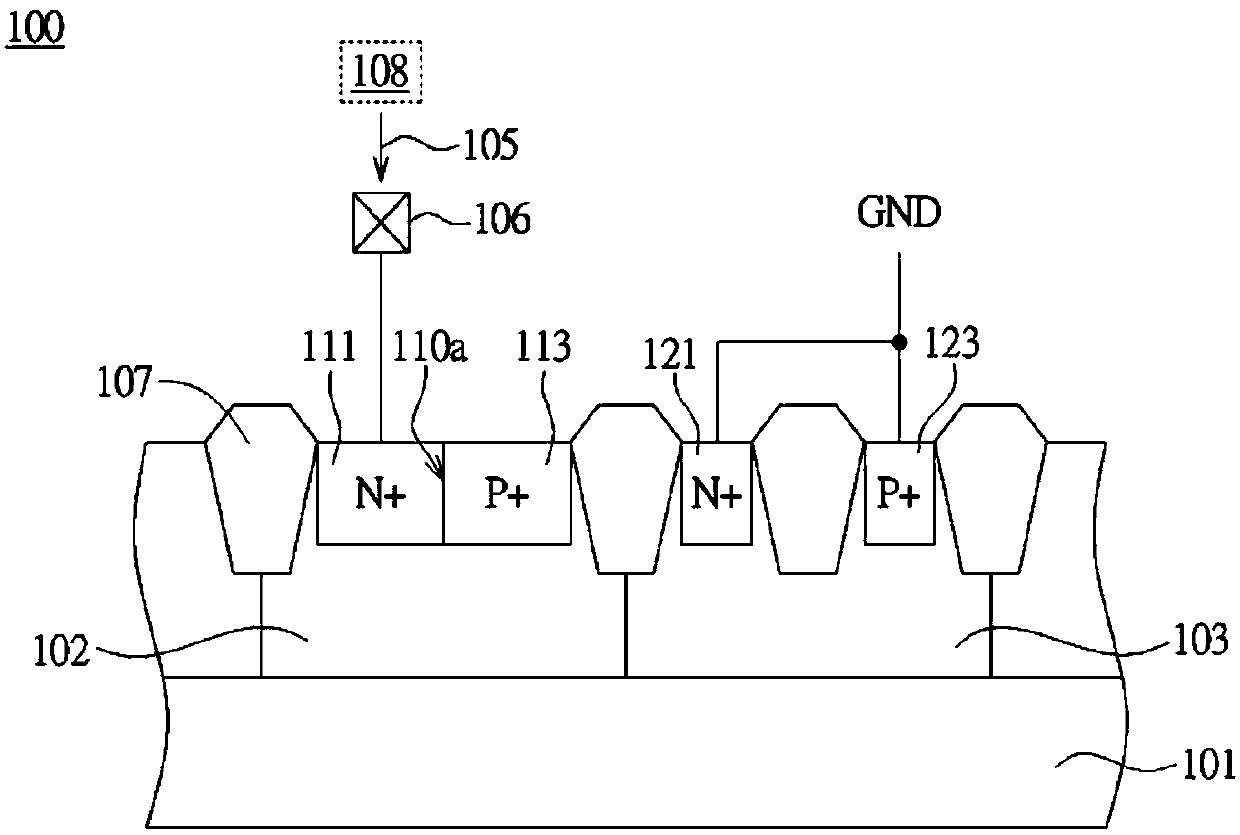
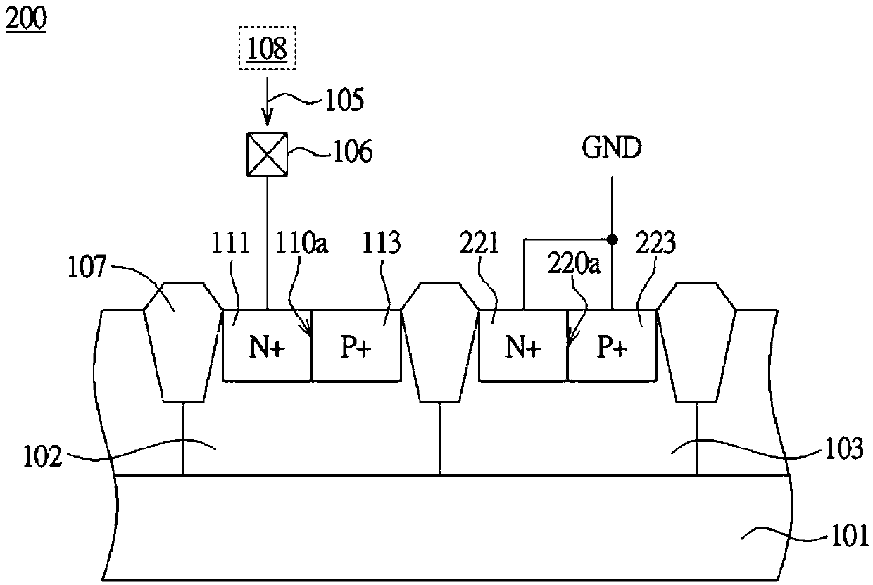
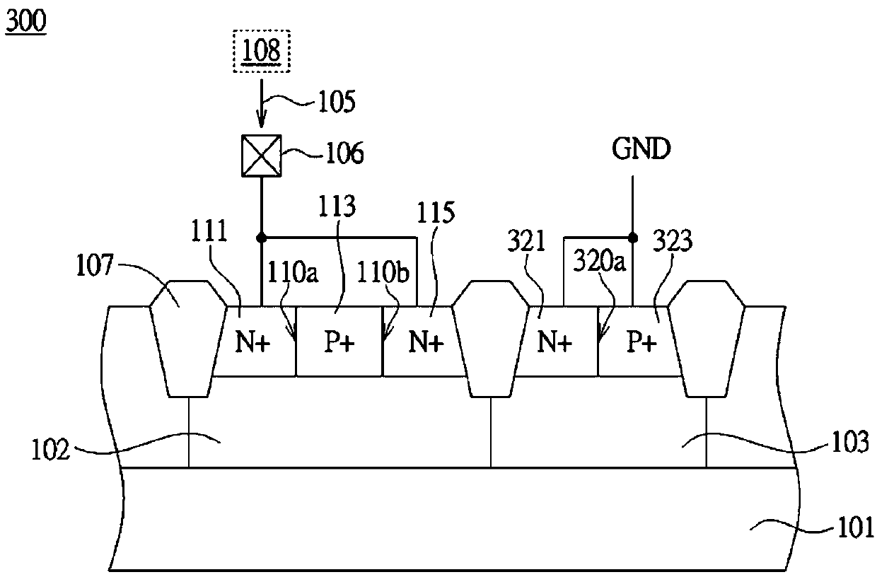
[0034] The disclosure provides an electrostatic discharge protection device and its application, which can solve the problem that the parasitic silicon controlled rectifier in the existing electrostatic discharge protection device is prone to power overload or latch-up. In order to make the above-mentioned embodiments and other objectives, features and advantages of the present disclosure more comprehensible, the following specifically cites several electrostatic discharge protection devices and their application methods and components as preferred embodiments, and describes in detail with the accompanying drawings.

[0035] However, it must be noted that these specific implementation cases and methods are not intended to limit this disclosure. The disclosure can still be implemented with other features, elements, methods and parameters. The preferred embodiments are presented only to illustrate the technical features of the present disclosure, not to limit the patent scope of...


PUM


Abstract

The invention provides an electrostatic discharge protection device. The protection device comprises a semiconductor substrate, a first well region, a second well region, a first doped region, a second doped region, a third doped region, a fourth doped region and at least one junction. The first well region and the second well region are located in the semiconductor substrate and have a first electrical property and a second electrical property respectively. The first doped region has a first electrical property and is located in the first well region. The second doped region has a second electrical property and is located in the first well region. The third doped region and the fourth doped region have a first electrical property and a second electrical property respectively and are located in the second well region. At least one junction is formed by different electrical properties and is formed by the first doped region and the second doped region or by the third doped region and the fourth doped region.

Description

technical field [0001] The invention relates to a semiconductor integrated circuit and its application. In particular, it relates to an electrostatic discharge (Electrostatic Discharge, ESD) protection device and an operating method thereof. Background technique [0002] Electrostatic discharge is caused by a powerful current pulse introduced by a high voltage discharge for a short period of time (typically within 100 nanoseconds). Integrated circuits and semiconductor components are quite sensitive to electrostatic discharge. Especially during component mounting, because humans or machines touch the pins, strong current pulses often pass through the integrated circuit, resulting in component failure. Therefore, there is a need to provide an effective ESD protection device for integrated circuits. [0003] A parasitic silicon controlled rectifier (Silicon Controlled Rectifier, SCR) is a chip (on-chip) semiconductor electrostatic discharge protection device, which can be t...

Claims


Application Information

Patent Timeline
IPC IPC(8): H01L27/02
CPCH01L27/0266
Inventor 王世钰李明颖
Owner MACRONIX INT CO LTD
Learn More