
Liquid crystal lens array device, imaging device and imaging method

A liquid crystal lens array and device technology, which is applied to instruments, nonlinear optics, optics, etc., can solve problems such as affecting the aperture ratio and excessive spacing, and achieve the effects of high aperture ratio, increased duty ratio, and improved imaging quality.

Active Publication Date: 2020-03-06
UNIV OF ELECTRONICS SCI & TECH OF CHINA
View PDF6 Cites 0 Cited by
  • Summary
  • Abstract
  • Description
  • Claims
  • Application Information

AI Technical Summary

Problems solved by technology

[0004] In view of this, an embodiment of the present invention provides a liquid crystal lens array device, an imaging device, and an imaging method to solve the problem in the prior art that the gap between adjacent microlenses in the liquid crystal lens array is too large to affect the aperture ratio.

Method used


Image

  • Liquid crystal lens array device, imaging device and imaging method
  • Liquid crystal lens array device, imaging device and imaging method
  • Liquid crystal lens array device, imaging device and imaging method

Examples


Embodiment 1

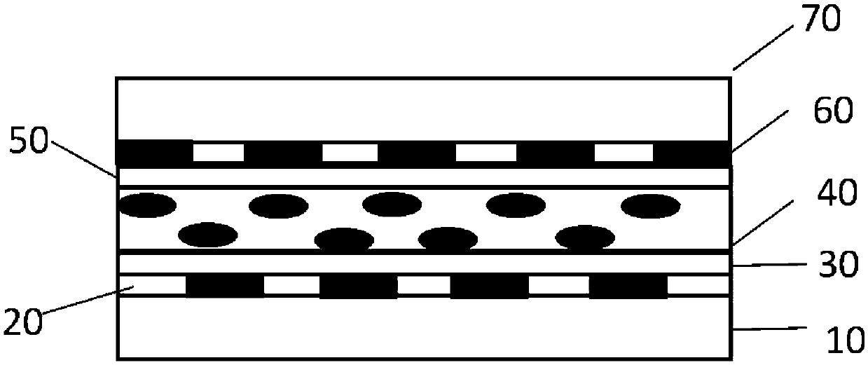
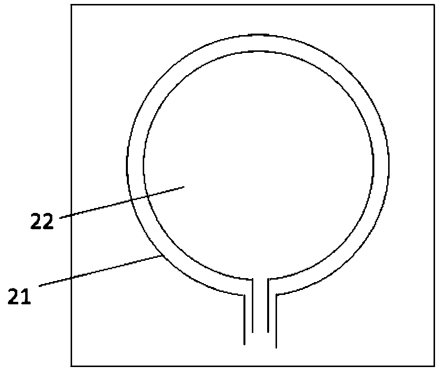
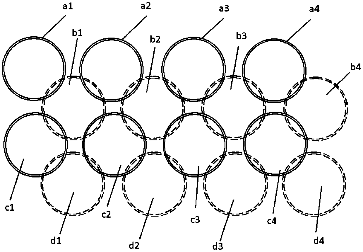
[0034] See figure 1 and figure 2 as well as image 3 , Embodiment 1 of the present invention provides a liquid crystal lens array device, its structure includes: first substrate 10, first array electrode 20, first alignment layer 30, liquid crystal layer 40, second alignment layer 50, second array electrode 60 and the second substrate 70. Wherein the first substrate 10 and the second substrate 70 are preferably glass substrates. Such as figure 2As shown, the first electrode array 20 includes a plurality of first electrode pairs 20 , and the first electrode pairs 20 are ring-shaped and include first electrodes 21 and second electrodes 22 . Likewise, the second electrode array 60 includes a plurality of second electrode pairs 60 , the second electrode pairs 60 are similar in shape to the first electrode pairs, and also have a ring shape, including third electrodes and fourth electrodes. Wherein the projection of the first electrode pair of the first array electrode 20 on ...

Embodiment 2

[0038] See Figure 4 and Figure 5 , the liquid crystal lens array device of the second embodiment of the present invention, compared with the liquid crystal lens array device of the first embodiment of the present invention, the main difference is that: two adjacent first electrodes of the first array electrode on the first substrate The pairs are tangent to each other, two adjacent second electrode pairs of the second array electrode on the second substrate are tangent to each other. Such as Figure 4 and Figure 5 , taking the first array electrode as an example, among the ring-shaped first electrode pairs a1, a2, a3 and a4 in the first row, any two adjacent first electrode pairs such as a1 and a2 are tangent to each other, and a1 and C1 among the ring-shaped second electrode pairs c1, c2, c3, and c4 in the adjacent second row is tangent, that is, each ring-shaped first electrode pair is in phase with the adjacent ring-shaped first electrode pair. cut. However, the pro...

Embodiment 3

[0044] See Figure 6 The main difference between Embodiment 3 of the present invention and Embodiment 1 of the present invention is that in Embodiment 3 of the present invention, a first transparent glass substrate (also called white glass) 80 is added between the first array electrode 20 and the first alignment layer 30, A second transparent glass substrate 90 is added between the second array electrodes 60 and the second alignment layer 50 . By arranging the first transparent glass substrate 80 and the second transparent glass substrate 90, when a voltage is applied to the first array electrode and the second array electrode, an inhomogeneous electric field distribution can be better formed, which is conducive to the formation of a gradient index electric field distribution, thereby improving the liquid crystal lens effect. The first transparent glass substrate and the second transparent glass substrate can be ordinary glass. By using the refractive index and insulating pro...


PUM


Abstract

The embodiment of the invention discloses a liquid crystal lens array device, an imaging device and an imaging method. The liquid crystal lens array device comprises a first array electrode, a secondarray electrode and a liquid crystal layer. The first array electrode comprises a plurality of first electrode pairs, the second array electrode comprises a plurality of second electrode pairs, the projections of the first electrode pairs of the first array electrode on a reference plane are partially overlapped with the second electrode pairs of the second array electrode, the reference plane isparallel to the plane of the liquid crystal layer, the first electrode pairs comprise first electrodes and second electrodes, the second electrode pairs comprise third electrodes and fourth electrodes, when a first liquid crystal lens array is formed at the T1 moment, the first electrodes apply first voltage, the second electrodes apply second voltage, and the second electrode pairs serve as common electrodes; when a second liquid crystal lens array is formed at the T2 moment, the third electrodes of the second electrode pairs apply first voltage, the fourth electrodes apply second voltage, and the first electrode pairs serve as common electrodes. The liquid crystal lens array device has the advantage of high duty ratio.

Description

technical field [0001] The invention relates to the technical field of optical imaging, in particular to a liquid crystal lens array device, an imaging device and an imaging method. Background technique [0002] Liquid crystal lens array is a kind of lens array based on liquid crystal material that has appeared in recent years. Liquid crystal is a good optoelectronic material with large optoelectronic anisotropy and birefringence. In recent years, it has been widely used in optical switches, wavefront detection, phase delay, optical fiber sensing and other fields. When the liquid crystal material is placed in an electric field or magnetic field, its molecular direction will be deflected by a certain angle with the strength of the electric field or magnetic field at the position. Utilizing this characteristic, by applying an inhomogeneous electric field, a gradient index lens is formed to perform operations such as convergence, divergence, and zooming of incident light. The...

Claims


Application Information

Patent Timeline
Patent Type & Authority Applications(China)
IPC IPC(8): G02F1/13G02F1/1343G02F1/29
CPCG02F1/1313G02F1/134309G02F1/29
Inventor 叶茂陈晓西王思聪晁晨
Owner UNIV OF ELECTRONICS SCI & TECH OF CHINA
Learn More