
Storage unit and multi-port static random access memory

A technology of storage unit and storage module, which is applied in the semiconductor field and can solve the problems of increased power consumption of write operations, etc.

Active Publication Date: 2020-03-06
LOONGSON TECH CORP
View PDF9 Cites 1 Cited by
  • Summary
  • Abstract
  • Description
  • Claims
  • Application Information

AI Technical Summary

Problems solved by technology

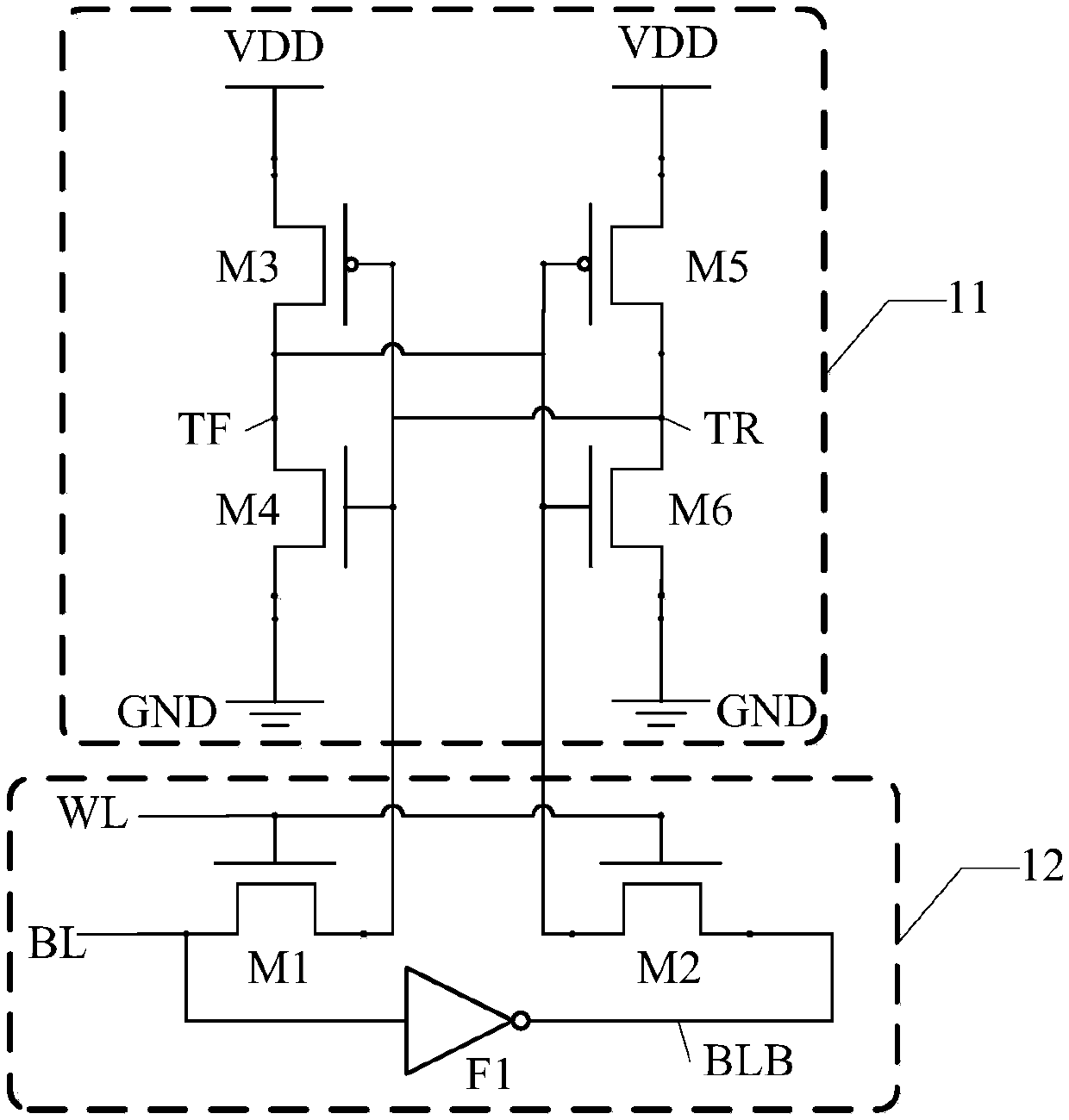
[0004] However, when the write operation occurs, if the signal input by the bit line BL is reversed, the signals on all the inverted bit lines BLB connected to the bit line BL are reversed, because only one write circuit 12 can be used for one storage circuit at a time. 11 for data writing, therefore, only the signal on one inverted bit line BLB is validly inverted, and the signals on the remaining inverted bit lines BLB are invalid inverted, resulting in increased power consumption caused by the write operation

Method used


Image

  • Storage unit and multi-port static random access memory
  • Storage unit and multi-port static random access memory
  • Storage unit and multi-port static random access memory

Examples


Embodiment 1

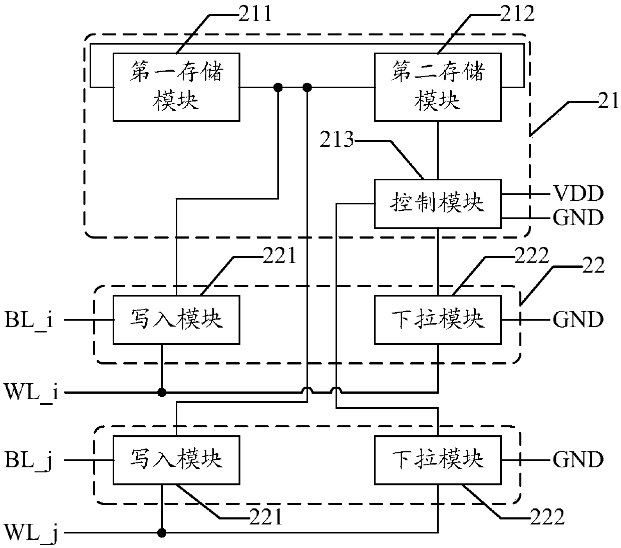
[0032] refer to figure 2 , shows a schematic structural diagram of a storage unit according to an embodiment of the present invention.

[0033] An embodiment of the present invention provides a storage unit, including: a storage circuit 21 and a plurality of writing circuits 22 .

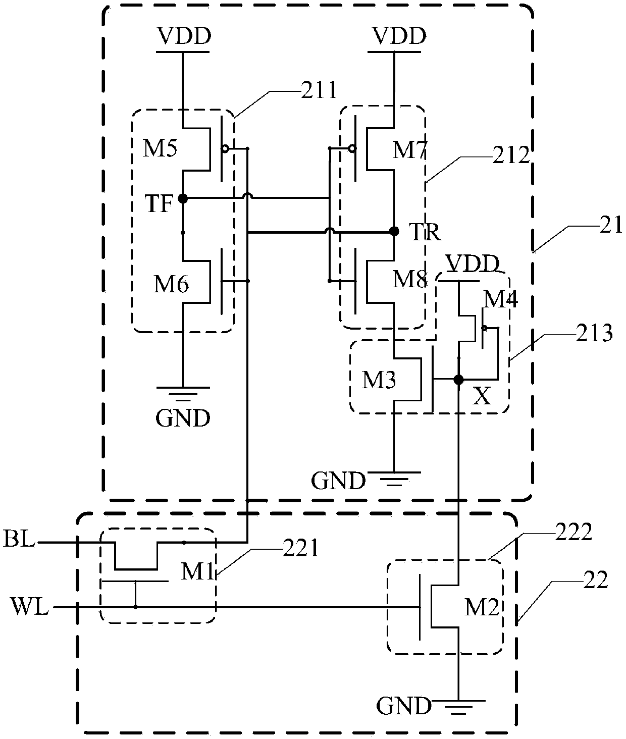
[0034] Wherein, the storage circuit 21 includes a first storage module 211, a second storage module 212 and a control module 213; the input terminal of the first storage module 211 is connected with the output terminal of the second storage module 212, and the output terminal of the first storage module 211 is connected with the output terminal of the second storage module 212. The input terminal of the second storage module 212 is connected; the control module 213 is respectively connected with the power supply voltage terminal VDD, the ground terminal GND and the second storage module 212, and is used to control the path between the output terminal of the second storage module 212 and the ground ...

Embodiment 2

[0077] An embodiment of the present invention also provides a multi-port SRAM, including the above storage unit.

[0078] Wherein, the multi-port SRAM includes a memory cell array, and the memory cell array includes a plurality of memory cells arranged in an array. When the multi-port SRAM includes n write ports, each memory cell includes a storage circuit 21 and n write circuits 22, the pin of each write port is connected to the word line WL and the bit line BL corresponding to each memory cell, for example, the pin of write port i is connected to the word line corresponding to each memory cell The line WL_i is connected to the bit line BL_i, and the pin of the write port j is connected to the word line WL_j corresponding to each memory cell and the bit line BL_j.

[0079] For the specific description of the storage unit, reference may be made to the description of Embodiment 1, which will not be repeated in this embodiment of the present invention.

[0080] In addition, the...


PUM


Abstract

The embodiment of the invention provides a storage unit and a multi-port static random access memory, and relates to the technical field of semiconductors. According to the embodiment of the invention, a storage circuit and a plurality of write-in circuits are arranged in the storage unit; the storage circuit comprises a first storage module, a second storage module and a control module. The control module is connected with a power supply voltage end, a grounding end and the second storage module, each write-in circuit comprises a write-in module and a pull-down module, the write-in module isconnected with a word line, a bit line and the input end of the first storage module, and the pull-down module is connected with the word line, the grounding end and the control module. By removing inverters and the reverse bit lines BLBs in the write-in circuits, when write-in operation occurs, extra power consumption caused by signal inversion on the reverse bit lines BLBs is avoided, and powerconsumption caused by the write-in operation is reduced; and when the signal input by the word line is valid, the path between the output end of the second storage module and the grounding end is disconnected, so that the reliability of writing operation is improved, and the writing difficulty is reduced.

Description

technical field [0001] The invention relates to the technical field of semiconductors, in particular to a storage unit and a multi-port static random access memory. Background technique [0002] SRAM (Static Random Access Memory, static random access memory), as an important type of IP (Intellectual Property, intellectual property) / macrocell, occupies an important position in integrated circuit design. With the continuous development and optimization of integrated circuit systems, The demand for the number of SRAM ports is gradually increasing, and multi-port SRAM provides important support for controllers, processors, etc. to store random / out-of-order instructions or data. [0003] like figure 1 As shown, each storage unit in the existing multi-port SRAM includes a storage circuit 11 and a plurality of write circuits 12, and the plurality of write circuits 12 include two N-type transistors (such as transistor M1 and transistor M2) and An inverter F1, the storage circuit 1...

Claims


Application Information

Patent Timeline
Patent Type & Authority Applications(China)
IPC IPC(8): G11C11/413
CPCG11C11/413
Inventor 丁健平王丽娜钟石强
Owner LOONGSON TECH CORP
Learn More