Novel perovskite and crystalline silicon back passivation laminated solar cell and manufacturing method thereof

A stacked solar and perovskite technology, which is applied in the fields of final product manufacturing, sustainable manufacturing/processing, semiconductor/solid-state device manufacturing, etc., to achieve the effect of improving conversion efficiency, steep absorption edge, and high photoelectric conversion efficiency

Pending Publication Date: 2020-03-06
RISEN ENERGY (CHANGZHOU) CO LTD
View PDF6 Cites 14 Cited by
  • Summary
  • Abstract
  • Description
  • Claims
  • Application Information

AI Technical Summary

Problems solved by technology

At present, the highest efficiency of the battery with this structure is the N-type battery created by the Fraunhofer Institute fo

Method used


Image

  • Novel perovskite and crystalline silicon back passivation laminated solar cell and manufacturing method thereof

Examples


Embodiment 1

[0033] This embodiment provides a method for manufacturing a novel solar cell based on perovskite and crystalline silicon rear passivation tandem solar cell and a novel tandem solar cell based on perovskite and crystalline silicon rear passivation manufactured by the method.

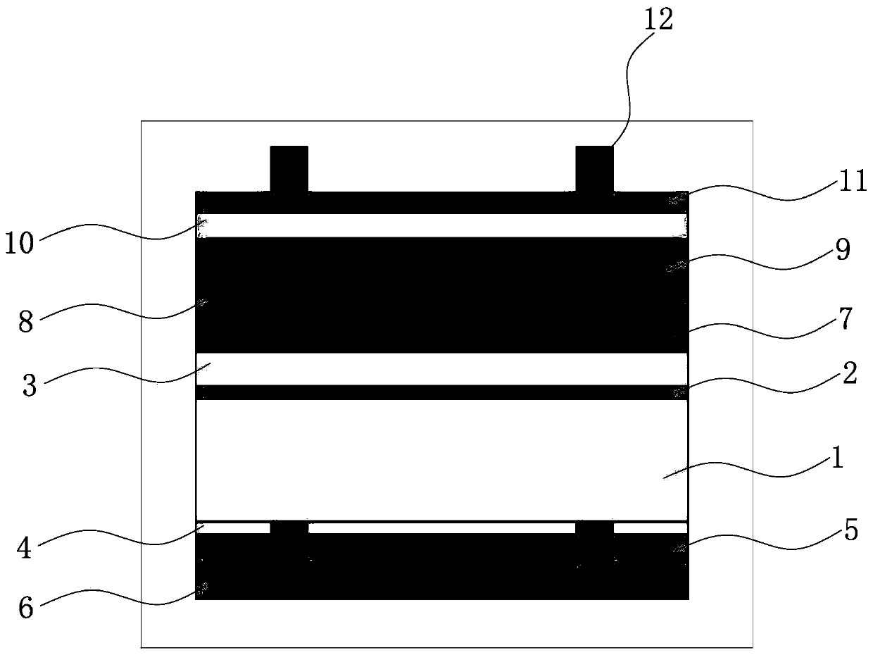
[0034] Such as figure 1 As shown, a novel method for preparing a stacked solar cell based on perovskite and crystalline silicon back passivation includes the following steps:

[0035] Step 1: Texturing, using a P-type monocrystalline silicon wafer as a silicon substrate, placing it in a texturing solution for texturing treatment, the texturing solution used is based on the mass ratio KOH:texturing additive:H 2 The ratio of O=20:3:160 is prepared, the temperature is 80°C, and then it is cleaned in hydrofluoric acid with a mass fraction of 5%, and the surface of the silicon chip is cleaned to obtain a P-type silicon substrate 1. The texturizing additive here is It refers to the addition of chemical additi...

Embodiment 2

[0048] This embodiment provides a method for manufacturing a novel solar cell based on perovskite and crystalline silicon rear passivation tandem solar cell and a novel tandem solar cell based on perovskite and crystalline silicon rear passivation manufactured by the method.

[0049] Such as figure 1 As shown, a novel method for preparing a stacked solar cell based on perovskite and crystalline silicon back passivation includes the following steps:

[0050] Step 1: Texturing, using a P-type monocrystalline silicon wafer as a silicon substrate, placing it in a texturing solution for texturing treatment, the texturing solution used is based on the mass ratio KOH:texturing additive:H 2 The ratio of O=20:3:160 is prepared, the temperature is 80° C., and then cleaned in hydrofluoric acid with a mass fraction of 2%, the surface of the silicon wafer is cleaned, and a P-type silicon substrate 1 is obtained;

[0051] Step 2: film deposition, using LPCVD equipment or PECVD equipment to...

Embodiment 3

[0061] This embodiment provides a method for manufacturing a novel solar cell based on perovskite and crystalline silicon rear passivation tandem solar cell and a novel tandem solar cell based on perovskite and crystalline silicon rear passivation manufactured by the method.

[0062] Such as figure 1 As shown, a novel method for preparing a stacked solar cell based on perovskite and crystalline silicon back passivation includes the following steps:

[0063] Step 1: Texturing, using a P-type monocrystalline silicon wafer as a silicon substrate, placing it in a texturing solution for texturing treatment, the texturing solution used is based on the mass ratio KOH:texturing additive:H 2 The ratio of O=20:3:160 is prepared, the temperature is 80° C., and then cleaned in hydrofluoric acid with a mass fraction of 4%, the surface of the silicon wafer is cleaned, and the P-type silicon substrate 1 is obtained;

[0064] Step 2: thin film deposition, using LPCVD equipment or PECVD equip...


PUM

PropertyMeasurementUnit
Thicknessaaaaaaaaaa
Bandgapaaaaaaaaaa
Thicknessaaaaaaaaaa

Abstract

The invention belongs to the technical field of solar cell preparation, and particularly relates to a novel perovskite and crystalline silicon back passivation laminated solar cell and a manufacturingmethod thereof. The solar cell includes a bottom cell and a top cell. An upper electrode is fixedly connected to the top cell. An intermediate layer is arranged between the bottom cell and the top cell. The bottom cell is a crystalline silicon back passivated cell. The intermediate layer is a transparent conductive film. The top cell is a perovskite cell. In the present invention, the silicon cell is used as the bottom cell, and the perovskite cell is used as the top cell. The band gap of the silicon cell is 1.12 eV, and the band gap of the perovskite cell is 1.65 to 1.7 eV. In cooperation with the bottom and top cells having such band gaps, the laminated solar cell has a high photoelectric conversion efficiency. In addition, the perovskite has a high absorption coefficient and a steep absorption edge so as to be suitable for the top cell of the crystalline silicon laminated solar cell.

Description

technical field [0001] The invention belongs to the technical field of solar cell manufacturing, and in particular relates to a novel laminated solar cell based on perovskite and crystalline silicon back passivation and a manufacturing method thereof. Background technique [0002] Solar energy technology is one of the hottest and most cutting-edge researches at present, but to replace traditional energy sources and truly realize a clean and renewable energy economy, its price needs to be further reduced, and one of the most effective ways to reduce costs is to increase the battery capacity. Photoelectric conversion efficiency. One of the most effective ways to improve photoelectric efficiency is to build a stacked solar cell system, that is, to stack several photovoltaic materials with different bandgap widths to form a multi-junction cell. Usually, the high-bandgap cell is placed on the top, and the low-bandgap cell is placed on the top. The width battery is placed on the ...

Claims


Application Information

Patent Timeline
IPC IPC(8): H01L51/42H01L51/48H01L31/0687H01L31/18
CPCH01L31/0687H01L31/1804H10K30/151H10K30/15H10K30/152Y02E10/544Y02E10/547Y02E10/549Y02P70/50
Inventor 万义茂胡玉婷崔艳峰袁声召庄宇峰黄强林海峰
Owner RISEN ENERGY (CHANGZHOU) CO LTD
Why Eureka
Try Eureka