Array substrate, preparation method thereof and display panel

A technology of array substrate and array layer, applied in semiconductor/solid-state device manufacturing, electrical components, electric solid-state devices, etc., can solve problems such as difficult-to-drive transistor drive capability, switch transistor control capability, etc.

Active Publication Date: 2020-03-13
YUNGU GUAN TECH CO LTD
View PDF4 Cites 6 Cited by
  • Summary
  • Abstract
  • Description
  • Claims
  • Application Information

AI Technical Summary

Problems solved by technology

[0004] However, it is difficult to simultaneously optimize the driving capability of the driving transistor and t

Method used


Image

  • Array substrate, preparation method thereof and display panel
  • Array substrate, preparation method thereof and display panel
  • Array substrate, preparation method thereof and display panel

Examples


Embodiment Construction

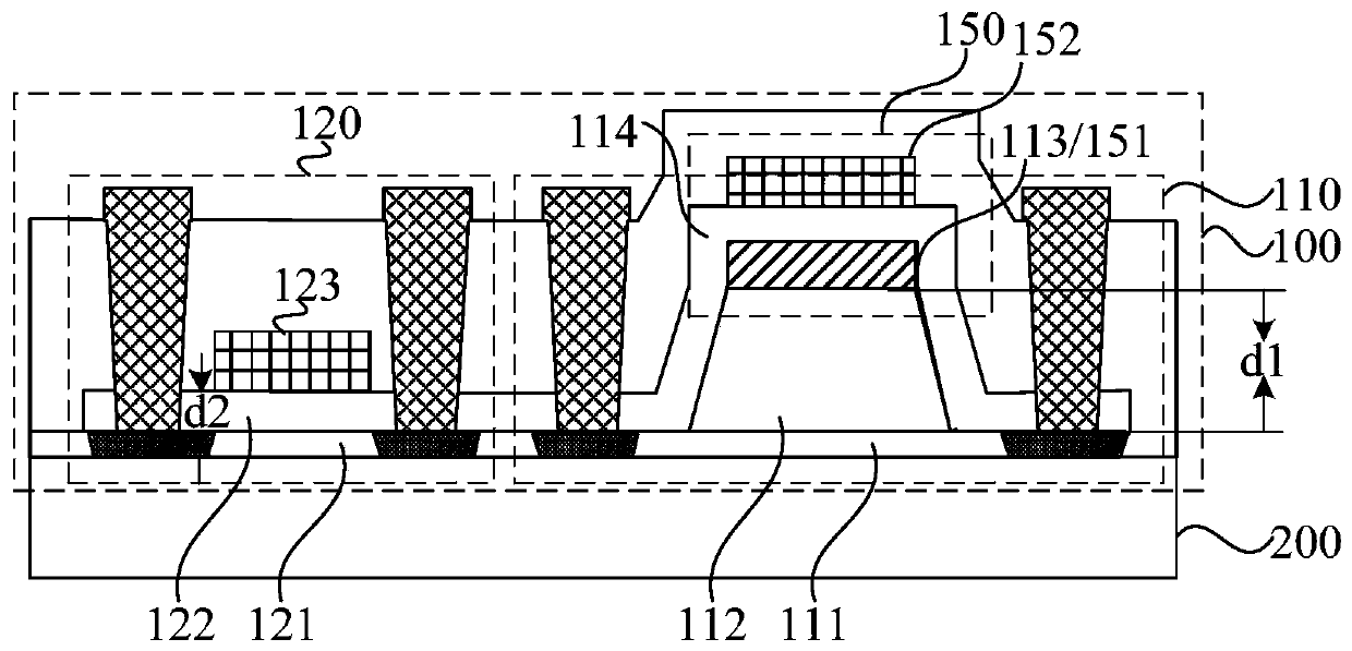
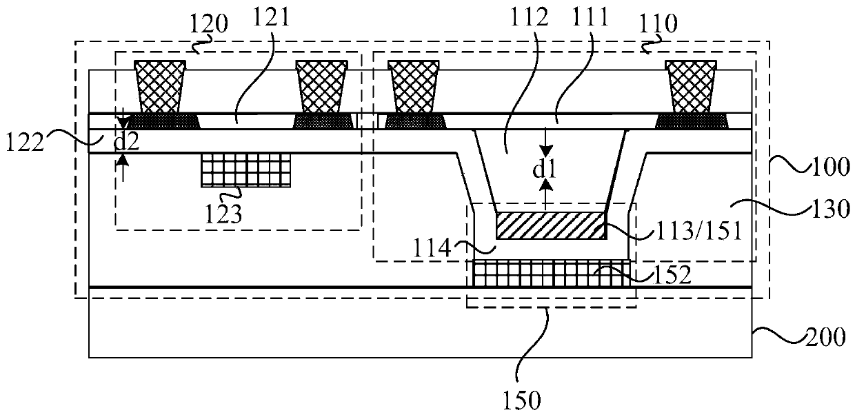
[0042] The present invention will be further described in detail below in conjunction with the accompanying drawings and embodiments. It should be understood that the specific embodiments described here are only used to explain the present invention, but not to limit the present invention. In addition, it should be noted that, for the convenience of description, only some structures related to the present invention are shown in the drawings but not all structures.

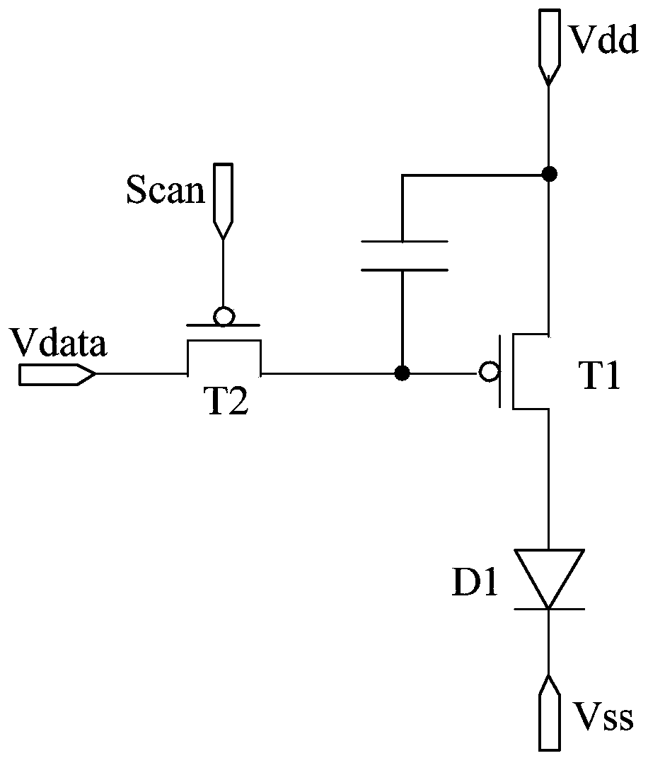
[0043] As mentioned in the background, it is difficult to simultaneously optimize the driving capability of the driving transistor and the control capability of the switching transistor in the structure of the existing organic light emitting display panel. The inventors have found through research that the reason for the above problems is that in the existing organic light-emitting display panels, the driving transistor and the switching transistor in the array substrate usually have the same device structure, spec...


PUM

PropertyMeasurementUnit
Thicknessaaaaaaaaaa
Thicknessaaaaaaaaaa

Abstract

The embodiment of the invention discloses an array substrate, a preparation method thereof and a display panel, the array substrate comprises a thin film transistor array layer, and the thin film transistor array layer comprises a driving transistor, a switching transistor and a capacitor; wherein the driving transistor comprises a first active layer, a first gate insulating layer, a first gate and an insulating dielectric layer which are stacked in sequence; the switching transistor comprises a second active layer, a second gate insulating layer and a second gate which are sequentially stacked; wherein the insulating dielectric layer and the second gate insulating layer are the same layer; the thickness of the first gate insulating layer is larger than that of the second gate insulating layer, so that the sub-threshold swing of the driving transistor is large, meanwhile, the sub-threshold swing of the switching transistor is small, and the driving capacity of the driving transistor and the switching control capacity of the switching transistor can be guaranteed at the same time.

Description

technical field [0001] Embodiments of the present invention relate to the field of display technology, and in particular, to an array substrate, a manufacturing method thereof, and a display panel. Background technique [0002] With the development of display technology, organic light emitting display panels are more and more widely used. [0003] Existing organic light-emitting display panels usually include a plurality of organic light-emitting devices and a driving circuit for driving the organic light-emitting devices to emit light, and the driving circuit usually includes a driving transistor and a switching transistor. [0004] However, it is difficult to simultaneously optimize the driving capability of the driving transistor and the control capability of the switching transistor in the existing organic light emitting display panel structure. Contents of the invention [0005] Embodiments of the present invention provide an array substrate, a manufacturing method t...

Claims


Application Information

Patent Timeline
IPC IPC(8): H01L27/12H01L27/32H01L21/84
CPCH01L27/1237H01L27/1259H10K59/1213
Inventor 赵东方文国哲李俊峰杜哲葛泳原莎徐琳
Owner YUNGU GUAN TECH CO LTD
Why Eureka
Try Eureka