A 12T TFET SRAM cell circuit having ultra-low power consumption and high write margin

A unit circuit, ultra-low power technology, applied in information storage, static memory, digital memory information, etc., can solve the problem that 6TTFETSRAM cells are difficult to achieve read, write and hold functions at the same time, unable to perform read operations, and high static power consumption, etc. problem, to achieve the effect of improving write margin and stability, improving stability and writing capability, and solving large static power consumption

Pending Publication Date: 2019-04-19
ANHUI UNIVERSITY
View PDF0 Cites 5 Cited by
  • Summary
  • Abstract
  • Description
  • Claims
  • Application Information

AI Technical Summary

Problems solved by technology

At present, papers and experiments have shown that due to the unidirectional conduction characteristics of TFETs, it is difficult for the traditional structure of 6T TFET SRAM cells to achieve ideal read, write and hold functions at the same time.
The OA-6T structure has very good writing ability, but the reading ability is very poor, and even the reading operation cannot be performed
[0005] figure 2 The 8T TFET SRAM (marked as DP-8T) structure and image 3 Although the 10T TFET SRAM (denoted as ST-10T) structure of the Schmitt-Trigger structure shown solves the problem of weak reading ability of the OA-6T structure, due to the positive bias leakage generated when the TFET is used as the SRAM transmission tube to maintain the equal state current will cause its static power dissipation to be large

Method used


Image

  • A 12T TFET SRAM cell circuit having ultra-low power consumption and high write margin
  • A 12T TFET SRAM cell circuit having ultra-low power consumption and high write margin
  • A 12T TFET SRAM cell circuit having ultra-low power consumption and high write margin

Examples


Embodiment Construction

[0026] The technical solutions in the embodiments of the present invention are clearly and completely described below in conjunction with the accompanying drawings in the embodiments of the present invention. Obviously, the described embodiments are only some of the embodiments of the present invention, not all of them. Based on the embodiments of the present invention, all other embodiments obtained by persons of ordinary skill in the art without making creative efforts belong to the protection scope of the present invention.

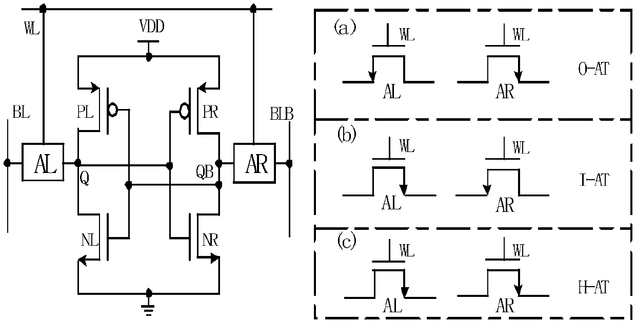
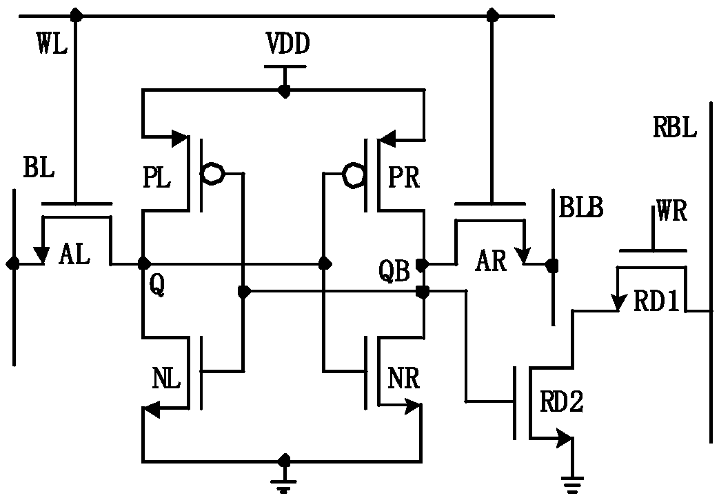
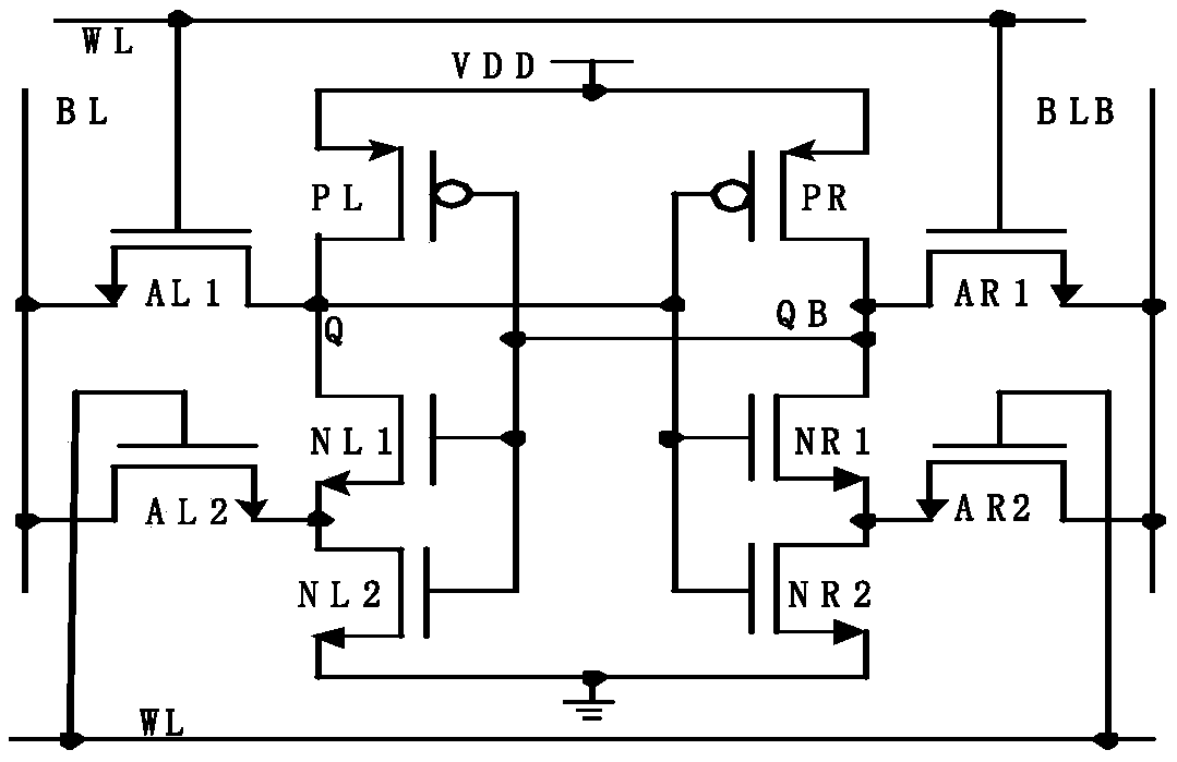
[0027] The basic device used in the traditional SRAM memory unit circuit is a MOSFET, and the basic device used in the Pro-12T unit circuit proposed by the present invention is a tunneling field effect transistor (TFET). When the TFET is used as the SRAM transmission tube in the hold state, the forward bias leakage current caused by its forward bias voltage will increase the static power consumption of the SRAM. At the same time, due to the unidirectio...


PUM


Abstract

The invention discloses a 12T TFET SRAM unit circuit with ultra-low power consumption and high write margin. Compared with a metal oxide semiconductor field effect transistor (MOSFET), the characteristics of smaller subthreshold swing, higher switching ratio and the like of the TFET are utilized; the problem of high static power consumption of a traditional MOSFET SRAM unit structure is solved; Under the same working voltage, such as 0.3 V to 0.6 V, compared with other TFET SRAM unit structures, the static power consumption of the TFET SRAM unit structure is at least reduced by four orders ofmagnitudes, and the write margin and the stability of the TFET SRAM unit structure are improved; Therefore, the problem of positive bias leakage current occurring when the TFET is used as the SRAM transmission tube is eliminated, the static power consumption of the cell is reduced, and the stability and the writing capability of the cell are improved.

Description

technical field [0001] The invention relates to the field of integrated circuit design, in particular to a 12T TFETSRAM unit circuit with ultra-low power consumption and high write margin. Background technique [0002] With the development of mobile electronic products, people's demand for low power consumption of integrated circuits has become more and more urgent. In recent years, MOSFET (Metal-Oxide Semiconductor Field Effect Crystal) has become an important part of digital integrated circuits and analog integrated circuits. However, with the development of integrated circuit technology nodes, some shortcomings of MOSFETs in ultra-low power circuits make it difficult to obtain satisfactory results. Because as the size of the MOSFET decreases, the short channel effect of the MOSFET weakens its ability to turn off at sub-threshold voltage, which increases the static leakage current and static power consumption of the circuit. In addition, the subthreshold swing of MOSFET ...

Claims


Application Information

Patent Timeline
Patent Type & Authority Applications(China)
IPC IPC(8): G11C11/402
CPCG11C11/4023
Inventor 卢文娟董兰志彭春雨吴秀龙蔺智挺陈军宁
Owner ANHUI UNIVERSITY
Why Eureka
Try Eureka