Organic light-emitting display device and manufacturing method thereof

A light-emitting display and organic technology, which is applied in semiconductor/solid-state device manufacturing, semiconductor devices, electrical components, etc., can solve the problems of not being able to satisfy electrical properties at the same time, and achieve the effect of rapid opening and closing

Active Publication Date: 2017-01-04
TCL CHINA STAR OPTOELECTRONICS TECH CO LTD
View PDF3 Cites 6 Cited by
  • Summary
  • Abstract
  • Description
  • Claims
  • Application Information

AI Technical Summary

Problems solved by technology

[0006] Aiming at the problem in the prior art that the subthreshold swings of the IdVg curves of the two thin film field effect transistors of the active matrix organic light emitting diode are almost the same and cannot meet the electrical requirements of each at the same time, the present invention proposes an organic light emitting display device and its manufacturing method

Method used


Image

  • Organic light-emitting display device and manufacturing method thereof
  • Organic light-emitting display device and manufacturing method thereof
  • Organic light-emitting display device and manufacturing method thereof

Examples


Embodiment 1

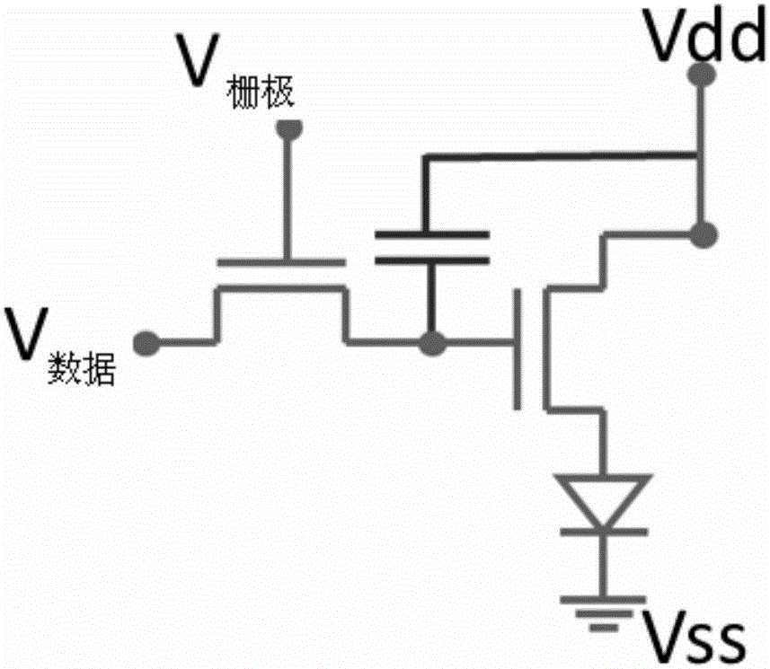
[0041] Figure 4 A schematic cross-sectional structure diagram of an organic light-emitting display device according to an embodiment of the present invention is shown. Such as Figure 4 As shown, the organic light emitting display device of this embodiment includes a switching TFT T1, a driving TFT T2, and a storage capacitor connected to the switching TFT T1 and the driving T2 respectively.

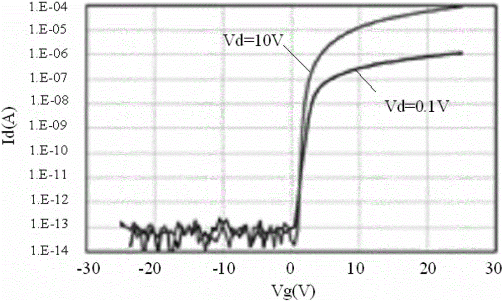
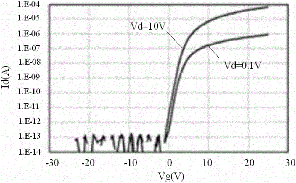
[0042] Specifically, the switching TFT T1 has a first active layer 9 for reducing the sub-threshold swing of the transfer characteristic curve of the switching TFT T1. Furthermore, the driving thin film field effect transistor T2 has a second active layer 10 for increasing the sub-threshold swing of the transfer characteristic curve of the driving thin film field effect transistor T2.

[0043] The first active layer 9 can make the sub-threshold swing of the transfer characteristic curve of the switching thin film field effect transistor T1 smaller, so that the switching thin film fiel...

Embodiment 2

[0046] The organic light-emitting display device of this embodiment includes a switching TFT T1, a driving TFT T2, and storage capacitors respectively connected to the switching TFT T1 and the driving T2.

[0047] Specifically, the switching TFT T1 has a first active layer 9 for reducing the sub-threshold swing of the transfer characteristic curve of the switching TFT T1. Furthermore, the driving thin film field effect transistor T2 has a second active layer 10 for increasing the sub-threshold swing of the transfer characteristic curve of the driving thin film field effect transistor T2.

[0048] Compared with Embodiment 1, the oxygen content of the second active layer 10 of the organic light emitting display device of this embodiment is higher than the oxygen content of the first active layer 9 . The oxygen content of the first active layer 9 determines the subthreshold swing of the transfer characteristic curve of the switching thin film field effect transistor T1, and the o...

Embodiment 3

[0051] The organic light-emitting display device of this embodiment includes a switching TFT T1, a driving TFT T2, and storage capacitors respectively connected to the switching TFT T1 and the driving T2.

[0052] Specifically, the switching TFT T1 has a first active layer 9 for reducing the sub-threshold swing of the transfer characteristic curve of the switching TFT T1. Furthermore, the driving thin film field effect transistor T2 has a second active layer 10 for increasing the sub-threshold swing of the transfer characteristic curve of the driving thin film field effect transistor T2. Wherein, the oxygen content of the second active layer 10 is higher than that of the first active layer 9 .

[0053] Compared with Embodiment 2, both the first active layer 9 and the second active layer 10 of the organic light emitting display device of this embodiment are InGaZnO compound layers.

[0054] The active layer requires high mobility of materials, but traditional amorphous silicon...


PUM


Abstract

The present invention discloses an organic light-emitting display device and a manufacturing method thereof. The organic light-emitting display device includes a switching thin film field effect transistor, a driving thin film field effect transistor, and a storage capacitor connected with the switching thin film field effect transistor and the driving thin film field effect transistor; the switching thin film field effect transistor is provided with a first active layer for reducing the subthreshold swing of the transfer characteristic curve of the switching film field effect transistor; and the driving thin film field effect transistor is provided with a second active layer for increasing the subthreshold swing of the transfer characteristic curve of the driving thin film field effect transistor. According to the organic light-emitting display device of the invention, fast switching on and switching off of the switching thin film field effect transistor and slow debugging of the grayscale of an OLED (Organic Light Emitting Diode) by the driving thin film field effect transistor can be simultaneously realized.

Description

technical field [0001] The present invention relates to the field of organic light emitting display technology, in particular to an organic light emitting display device, and also to a manufacturing method of the organic light emitting display device. Background technique [0002] Thin film field effect transistors based on semiconducting oxides are a hot topic in the future display field, and have been extensively researched and developed in recent years. The most basic structure of an active matrix organic light emitting diode (AMOLED) based on a thin film field effect transistor (TFT) is a 2T1C structure. Such as figure 1 As shown, the 2T1C structure consists of two thin film field effect transistors and a storage capacitor Cst between them. [0003] The mobility of the amorphous indium gallium zinc oxide (a-IGZO) film used as the active channel layer can be as high as 80cm 2 / Vs (the mobility of amorphous silicon is only 0.5-0.8cm 2 / Vs). In addition, the process of...

Claims


Application Information

Patent Timeline
Patent Type & Authority Applications(China)
IPC IPC(8): H01L27/32H01L51/56H01L21/77
CPCH01L21/77H10K59/88H10K59/00H10K71/00H01L29/66969H01L27/1225H01L29/78696H01L29/7869H01L27/1255H10K59/1213
Inventor 石龙强
Owner TCL CHINA STAR OPTOELECTRONICS TECH CO LTD
Why Eureka
Try Eureka