Array substrate, preparation method thereof, display panel and device

An array substrate and substrate substrate technology, which is applied in semiconductor/solid-state device manufacturing, electrical components, electrical solid-state devices, etc., can solve problems such as inability to meet display requirements, and achieve good turn-off characteristics, small sub-threshold swing, and high performance. good effect

Pending Publication Date: 2021-02-12
XIAMEN TIANMA MICRO ELECTRONICS
View PDF0 Cites 6 Cited by
  • Summary
  • Abstract
  • Description
  • Claims
  • Application Information

AI Technical Summary

Problems solved by technology

However, due to the different functions of the driving transistor and the switching transistor, the driving transistor and the switching transistor prepared by the same process often cannot meet the actual display requirements.

Method used


Image

  • Array substrate, preparation method thereof, display panel and device
  • Array substrate, preparation method thereof, display panel and device
  • Array substrate, preparation method thereof, display panel and device

Examples


preparation example Construction

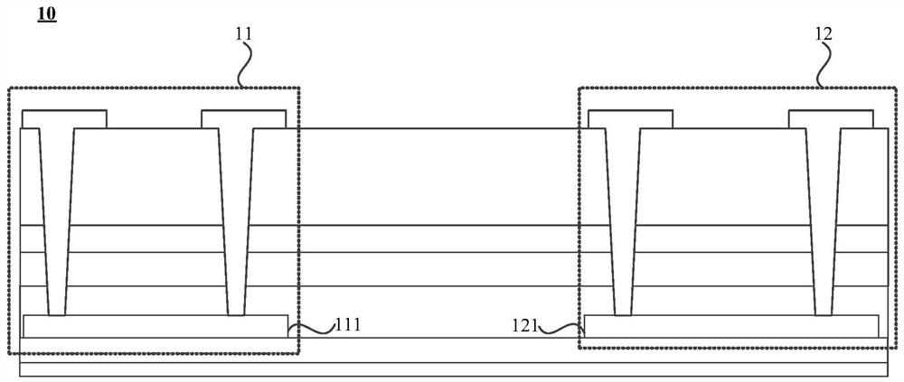
[0066] Based on the inventive concept at the same time, an embodiment of the present invention also provides a method for preparing an array substrate, which is used to prepare the array substrate described in the above embodiment, combining Figure 4 , Figure 5 , Image 6 , Figure 7 and Figure 8 As shown, the array substrate 20 includes a pixel circuit 22, the pixel circuit 22 includes a first transistor 221 and a second transistor 222, the first transistor 221 includes a first active layer 2211, the second transistor 222 includes a second active layer 2221, and the second transistor 222 includes a second active layer 2221. Both the first active layer 2211 and the second active layer 2221 include silicon. Figure 10 is a schematic flowchart of a method for preparing an array substrate provided by an embodiment of the present invention, as shown in Figure 10 As shown, the preparation method of the array substrate provided by the embodiment of the present invention incl...


PUM


Abstract

The invention discloses an array substrate, a preparation method thereof, a display panel and a device. The array substrate comprises a pixel circuit, the pixel circuit comprises a first transistor and a second transistor, the first transistor comprises a first active layer, the second transistor comprises a second active layer, and both the first active layer and the second active layer comprisesilicon; the array substrate further comprises a first type inorganic layer, a second type inorganic layer and a first via hole, the first via hole is located above the first active layer and at leastpenetrates through the second type inorganic layer, and the hydrogen ion concentration in the first active layer is smaller than that in the second active layer. The first active layer is subjected to high-temperature processing through the first via hole, so that the hydrogen ion concentration in the first active layer is smaller than that in the second active layer, the high-temperature processing frequency of the second transistor is reduced while good performance of the first transistor is guaranteed, and it is guaranteed that the second transistor is small in sub-threshold swing, good inturn-off characteristic and small in leakage current; and good overall characteristics of the pixel circuit are ensured.

Description

technical field [0001] Embodiments of the present invention relate to the field of display technology, and in particular to an array substrate and a manufacturing method thereof, a display panel and a device. Background technique [0002] Organic light-emitting display is currently the mainstream technology for displays such as mobile phones, TVs, and computers. Compared with traditional liquid crystal displays, organic light-emitting displays have the advantages of low energy consumption, low cost, self-illumination, wide viewing angle, and fast response speed. Therefore, organic light-emitting display gradually becomes a mainstream display technology. [0003] Since the organic light emitting display is driven by current, a stable current is required to control its light emission. The size and stability of the driving current of the organic light emitting display mainly depends on the driving transistor in the pixel circuit of the organic light emitting display. Therefor...

Claims


Application Information

Patent Timeline
Patent Type & Authority Applications(China)
IPC IPC(8): H01L27/12H01L27/32H01L21/77
CPCH01L27/1229H01L27/1248H01L27/1259H01L27/1225H10K59/1213H01L27/1222H10K59/1201H10K50/844H10K59/1216H10K71/00
Inventor 袁永
Owner XIAMEN TIANMA MICRO ELECTRONICS
Why Eureka
Try Eureka