A transistor structure with double buried oxide layer and its preparation method

A technology of double buried oxide layer and buried oxide layer is applied in the direction of transistor, semiconductor/solid-state device manufacturing, semiconductor device, etc., which can solve the problems that high-resistance substrate and back-gate voltage cannot be shared, difficult to perform high-performance radio frequency circuits, etc. Achieve the effects of harmonic suppression and crosstalk noise suppression, high RF characteristics, small substrate loss and crosstalk

Active Publication Date: 2021-11-05
SHANGHAI INST OF MICROSYSTEM & INFORMATION TECH CHINESE ACAD OF SCI
View PDF5 Cites 0 Cited by
  • Summary
  • Abstract
  • Description
  • Claims
  • Application Information

AI Technical Summary

Problems solved by technology

[0003] The purpose of the present invention is to provide a transistor structure with a double buried oxide layer and its preparation method, so as to solve the problem that the high-resistance substrate and the back gate voltage function cannot be shared in the prior art, so it is difficult to use the back gate voltage adjustment technology to realize high-performance radio frequency circuit problem

Method used


Image

  • A transistor structure with double buried oxide layer and its preparation method
  • A transistor structure with double buried oxide layer and its preparation method

Examples


Embodiment Construction

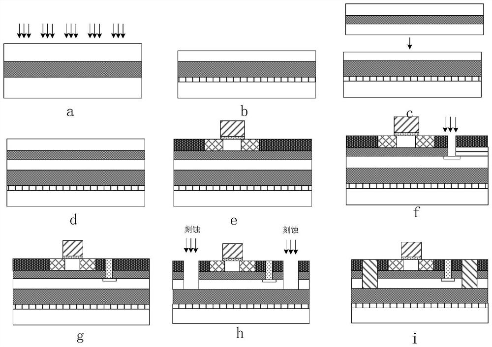
[0021] The present invention will be further described below in conjunction with specific embodiments. It should be understood that the following examples are only used to illustrate the present invention but not to limit the scope of the present invention.

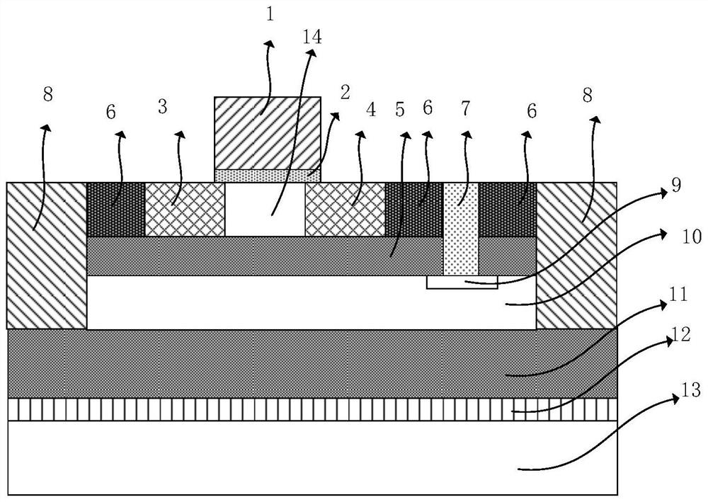
[0022] According to a preferred embodiment of the present invention, a transistor structure 100 with a double buried oxide layer is provided, such as figure 1 As shown, the transistor structure 100 includes in order from top to bottom: a top silicon layer 14, a gate 1 located above the top silicon layer 14, a gate dielectric layer 2, a source 3 and a drain 4 located at both lateral ends of the top silicon layer 14 , the shallow trench isolation region 6 located at the outer end of the active region; the first buried oxide layer 5 ; the second silicon layer 10 ; the second buried oxide layer 11 ; the defect layer 12 ; Wherein, the transistor structure 100 also includes a via hole 7 that sequentially penetrates the shallow...


PUM


Abstract

The invention provides a transistor structure with a double buried oxide layer and a preparation method thereof, comprising: a top silicon layer, an active region, and a shallow trench isolation region from top to bottom, and the active region includes: a top silicon layer located above The gate, the gate dielectric layer, the source and the drain located at the lateral ends of the top silicon layer; the first buried oxide layer; the second silicon layer; the second buried oxide layer; the substrate silicon layer; The isolation region, the through hole of the first buried oxide layer, the through hole is implanted or doped with particles, and an ohmic contact region is formed at the interface between the second silicon layer and the through hole; through the shallow trench isolation region, the first buried oxide layer in sequence layer and the deep trench isolation region formed by the second silicon layer; and a defect layer formed at the interface between the substrate silicon layer and the second buried oxide layer. The transistor structure provided by the invention can realize lower substrate loss and harmonic noise, so that the device can realize higher radio frequency characteristics under harsh conditions, and realize integration with digital circuits and analog circuits.

Description

technical field [0001] The invention relates to the technical field of semiconductor devices, in particular to a transistor structure with a double-buried oxide layer and a preparation method thereof. Background technique [0002] SOI technology (the full name of SOI is Silicon-On-Insulator, that is, silicon on insulating substrate, which is to introduce a buried oxide layer between the top silicon and the back substrate) has low power consumption, high speed, and anti-latch-up And excellent radio frequency performance and other characteristics, while SOI technology has excellent radiation resistance performance, and is widely used in the aerospace field. SOI technology is generally divided into two kinds of partial depletion and full depletion technology. For partially depleted SOI technology, a high-resistance substrate, such as HR SOI or TR SOI substrate, can be used to improve the radio frequency characteristics of the device and reduce harmonic noise. The fully deplet...

Claims


Application Information

Patent Timeline
Patent Type & Authority Patents(China)
IPC IPC(8): H01L29/06H01L29/78H01L21/336
CPCH01L29/0649H01L29/0684H01L29/66568H01L29/78
Inventor 吕凯董业民
Owner SHANGHAI INST OF MICROSYSTEM & INFORMATION TECH CHINESE ACAD OF SCI
Why Eureka
Try Eureka