High-speed level conversion circuit applied to mixed voltage output buffer

A technology of output buffer and conversion circuit, which is applied in the direction of logic circuit coupling/interface, logic circuit, and logic circuit interface device using field effect transistors, and can solve the problems of slow conversion speed and the like

Pending Publication Date: 2020-03-17
重庆中易智芯科技有限责任公司
View PDF0 Cites 1 Cited by
  • Summary
  • Abstract
  • Description
  • Claims
  • Application Information

AI Technical Summary

Problems solved by technology

A high-speed level conversion circuit applied to mixed voltage output buffers is proposed to sol...

Method used


Image

  • High-speed level conversion circuit applied to mixed voltage output buffer
  • High-speed level conversion circuit applied to mixed voltage output buffer
  • High-speed level conversion circuit applied to mixed voltage output buffer

Examples


Embodiment Construction

[0015] The technical solutions in the embodiments of the present invention will be described clearly and in detail below with reference to the drawings in the embodiments of the present invention. The described embodiments are only some of the embodiments of the invention.

[0016] The technical scheme that the present invention solves the problems of the technologies described above is:

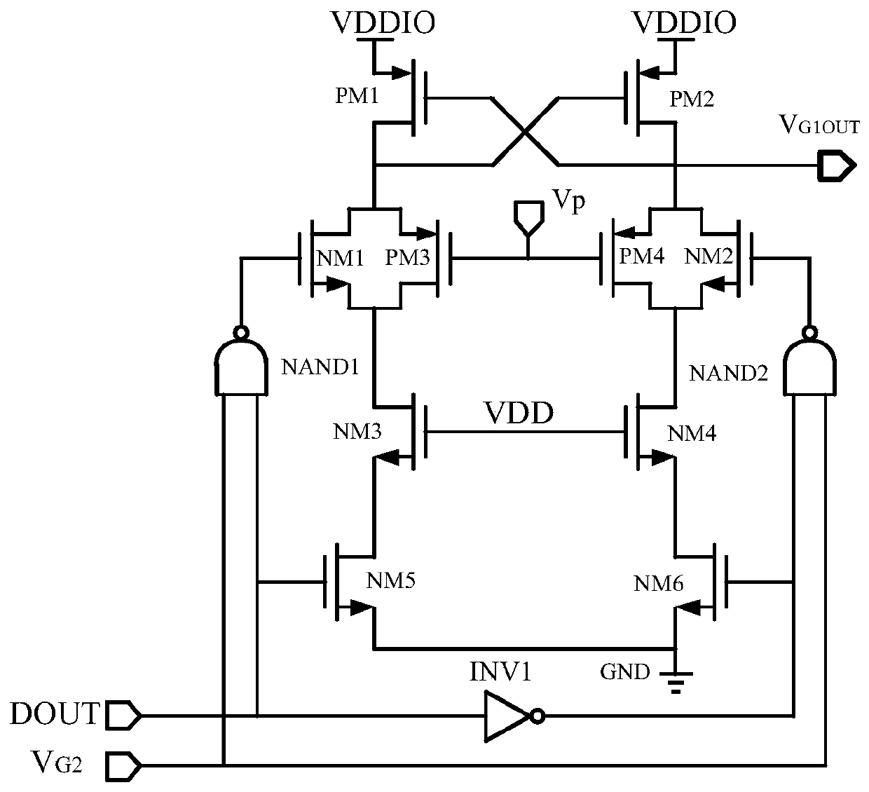
[0017] figure 1 Shown is a conventional mixed voltage level translation circuit. The circuit can realize the voltage conversion of VDDIO=VDD / 2*VDD, the input signal DOUT is the pulse signal for conversion and transmission, and VG2 is the judgment signal of the VDDIO voltage value. The circuit principle is as follows. In VDDIO=VDD mode, VG2 is logic "0", at this time, NMOS tubes NM1 and NM2 are kept on. When DOUT = "1", NM5 is on and NM6 is off, so the drain voltage of NM1 is GND. After turning on PM2, V G1OUT The voltage is VDDIO=VDD; similarly, when DOUT="0", NM5 is off and NM6 is on, s...


PUM


Abstract

The invention provides high-speed level conversion circuit applied to a mixed voltage output buffer. The circuit comprises a level conversion circuit and a VDDIO judgment circuit, and corresponding correct bias signals are provided for an output stage of the output buffer to drive a PMOS transistor in different voltage modes. VDDIO is the working mode voltage of the output buffer and can be VDD and 2 * VDD, DOUT is a pulse signal needing to be transmitted, and the VDDIO judgment circuit provides a control signal VG2 for the level conversion circuit according to the VDDIO voltage. In the VDD mode of the output buffer, VG2 is logic '0', PM3 and PM4 are closed, NM3 and NM4 are respectively conducted or closed according to the level state of DOUT, and 0-VDD pulse signals are output. In the 2 *VDD mode, VG2 is logic '1', PM3 and PM4 are switched on, NM3 and NM4 are switched off, and VDD-2 * VDD pulse signals are output. Voltage generation paths of different working modes of VDDIO are controlled through the logic gate so as to improve the speed of level conversion, and therefore the transmission frequency of the output buffer is improved.

Description

technical field [0001] The invention belongs to the technical field of integrated circuit design, and in particular relates to a high-speed level conversion circuit applied to a mixed voltage output buffer. Background technique [0002] With the improvement of process technology, chips manufactured by different processes may be integrated in the circuit system. In order to meet the requirements of signal transmission and reduce manufacturing costs, the mixed voltage mode output buffer is a good choice for signal transmission between modules. s solution. In a specific circuit system, such as a PCI system, DDR4, etc., there is a higher requirement for a signal transmission frequency. In the mixed voltage output buffer circuit, the low level is logic "0" in different voltage modes, and the NMOS gate terminal of the output stage is directly connected to the transmission signal. However, since there are two working modes of VDDIO=VDD / 2*VDD, the high levels are different, and th...

Claims


Application Information

Patent Timeline
IPC IPC(8): H03K19/0175H03K19/0185H03K19/017
CPCH03K19/017H03K19/017509H03K19/018507
Inventor 王巍赵元遥赵汝法袁军
Owner 重庆中易智芯科技有限责任公司
Why Eureka
Try Eureka