Phase dimming circuit and method
A dimming circuit and phase technology, applied in the field of phase dimming circuit and phase dimming, can solve problems affecting the grid environment, damage of power devices, periodic mutation of grid current, etc., and achieve the effect of prolonging life
- Summary
- Abstract
- Description
- Claims
- Application Information
AI Technical Summary
Problems solved by technology
Method used
Image

Examples
Embodiment Construction
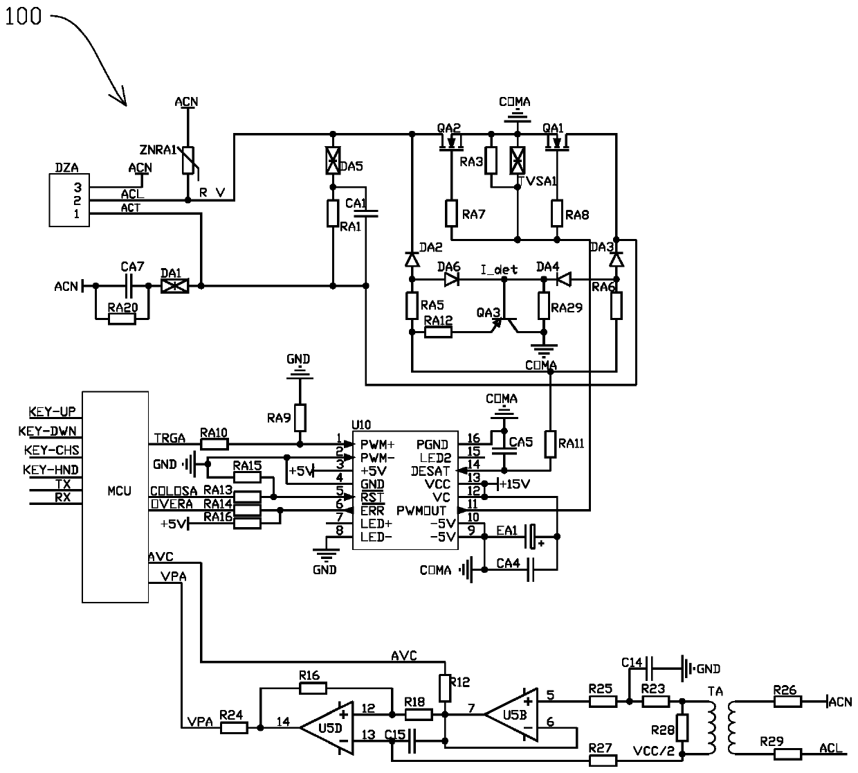
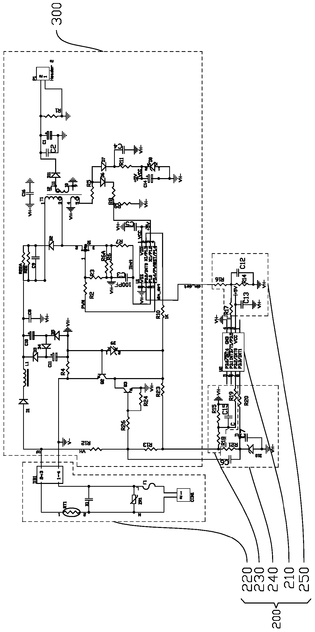
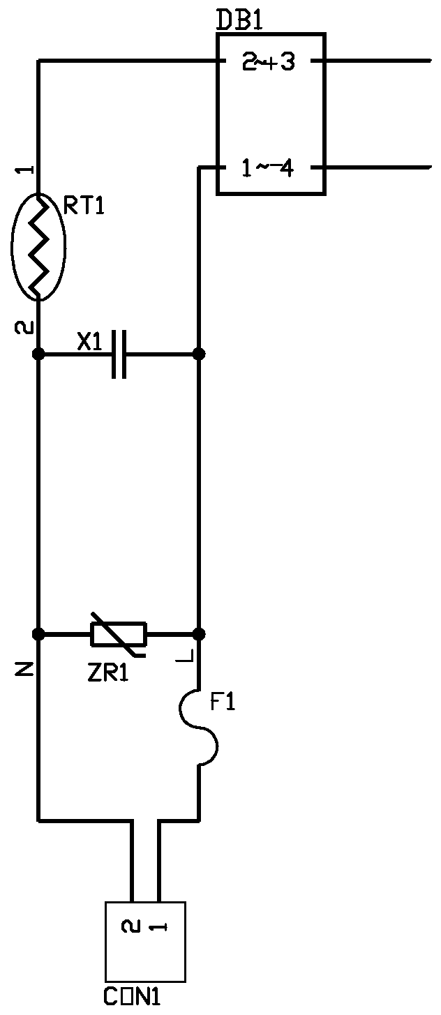
[0033] Embodiments of the present invention are described in detail below, examples of which are shown in the drawings, wherein the same or similar reference numerals designate the same or similar elements or elements having the same or similar functions throughout. The embodiments described below by referring to the figures are exemplary only for explaining the present invention and should not be construed as limiting the present invention.
[0034] In the description of the present invention, several means one or more, and multiple means more than two. Greater than, less than, exceeding, etc. are understood as not including the original number, and above, below, within, etc. are understood as including the original number. If the description of the first and second is only for the purpose of distinguishing the technical features, it cannot be understood as indicating or implying the relative importance or implicitly indicating the number of the indicated technical features or...
PUM
 Abstract
Description
Claims
Application Information
PatSnap Eureka turns technology decisions into work you can execute. Powered by our Innovation Knowledge Graph, it runs expert workflows across engineering, life sciences, materials and intellectual property. Get your review-ready output in minutes.


