Crimping type IGBT device structure optimization design method

A technology for optimizing design and device structure, applied in computer-aided design, design optimization/simulation, instrumentation, etc.

Active Publication Date: 2020-04-10
HUNAN CITY UNIV
View PDF2 Cites 2 Cited by
  • Summary
  • Abstract
  • Description
  • Claims
  • Application Information

AI Technical Summary

Problems solved by technology

Secondly, the IGBT device contains a large number of sub-modules, resulting in a large number of design variables in the structural optimization model. When solving, it is necessary to repeatedly call the multi-field coupling simulation model, which involves the high-dimensional structural optimization of the time-consuming simulation model. Solving is extremely challenging in terms of efficiency and convergence

Method used


Image

  • Crimping type IGBT device structure optimization design method
  • Crimping type IGBT device structure optimization design method
  • Crimping type IGBT device structure optimization design method

Examples


Embodiment Construction

[0079] Below in conjunction with embodiment, the present invention is described further, but does not constitute any restriction to the present invention, any limited number of modifications done in the scope of claims of the present invention is still within the scope of claims of the present invention.

[0080] Such as figure 1 — Figure 4 As shown, the present invention provides a method for optimizing the design of a crimped IGBT device structure, the method comprising the following processing steps:

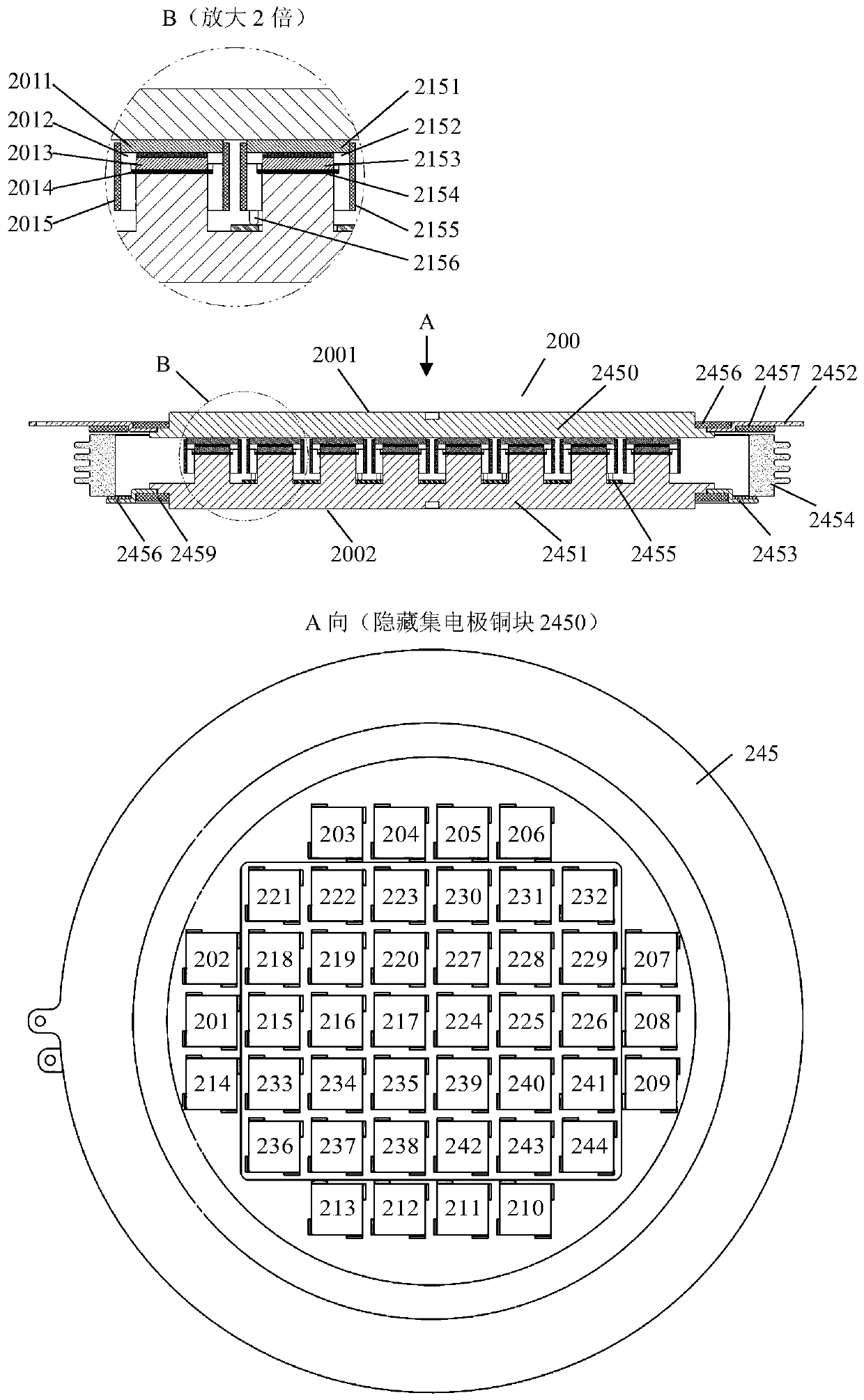
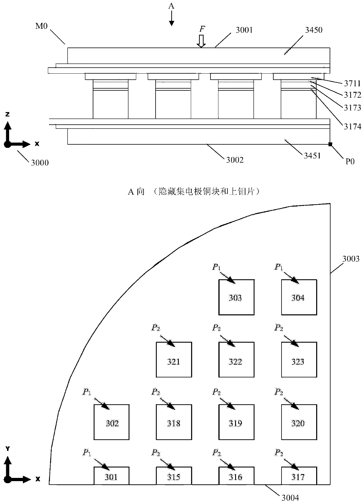
[0081] Step S1: Based on the press-connect IGBT device to be optimized, select a design target. Such as figure 2 As shown, the crimp-type IGBT device 200 in this embodiment is composed of a housing module 245 and 44 first sub-modules (201-244). The casing module 245 is composed of a collector copper block 2450 , an emitter copper block 2451 , a collector flange 2452 , an emitter flange 2453 , a tube shell 2454 , a circuit board 2455 , and insulating pads 2456-2459. The ...


PUM


Abstract

The invention relates to the technical field of high-power semiconductor device structure design. The invention discloses a crimping type IGBT device structure optimization design method, which comprises the following processing steps of selecting a design target based on a crimping type IGBT device to be optimized; based on the crimping type IGBT device, establishing a thermal coupling finite element analysis model M0, and further selecting a coupling temperature-displacement steady-state solver to solve the finite element analysis model M0; based on the position and the stress value of eachchip, establishing a stress balance coefficient response surface; forming an initial coefficient vector a (0) as an initial point, constructing an optimization model, and solving the optimization model to obtain an optimal coefficient vector a *; and constructing a silver sheet design scheme based on the optimal balance coefficient. Compared with the prior art, the structure optimization model established by the method can be solved on the basis of existing finite element analysis commercial software and a classical optimization algorithm, so that a tedious and complex programming process is avoided, and the method has good engineering usability.

Description

technical field [0001] The invention mainly relates to the technical field of structural design of high-power semiconductor devices, in particular to a method for optimizing the structural design of a pressure-connected IGBT device. Background technique [0002] The rapid development of voltage-flexible direct current transmission technology puts forward strict requirements on the capacity and reliability of power electronic devices in its core equipment. An insulated gate bipolar transistor (Insulated Gate Bipolar Transistor, IGBT) is one of the most typical types of fully-controlled voltage-driven power semiconductor devices. Compared with the traditional soldered IGBT module, the press-fit IGBT device has the advantages of double-sided heat dissipation, easy series connection, high power density and failure short-circuit working mode, and is very suitable for high-voltage and high-power application scenarios such as power systems. Press-fit IGBT can be roughly divided in...

Claims


Application Information

Patent Timeline
Patent Type & Authority Applications(China)
IPC IPC(8): G06F30/23G06F30/367G06F119/14
Inventor 黄志亮阳同光黎灿兵李文芳周理袁越阳
Owner HUNAN CITY UNIV
Why Eureka
Try Eureka