PCB defect detection method based on semantic segmentation

A PCB board and semantic segmentation technology, applied in the direction of optical testing flaws/defects, material analysis, image analysis, etc., can solve the problems of large manpower consumption, low detection efficiency, manual misjudgment, etc., achieve high-precision defect detection and reduce labor Effect of intervention, batch detection

Pending Publication Date: 2020-04-10
FOSHAN NANHAI GUANGDONG TECH UNIV CNC EQUIP COOP INNOVATION INST +1
View PDF0 Cites 7 Cited by
  • Summary
  • Abstract
  • Description
  • Claims
  • Application Information

AI Technical Summary

Problems solved by technology

[0002] For a long time, the quality problems of PCB board products caused by bumps and stains in the production process have attracted the attention of manufacturers. PCB defect detection is extremely important. With the continuous expansion of PCB market demand, its defect detection task has also changed. get harder
[0003] In the past, the traditional PCB board defect detection method has developed from manual screening to the automatic detection stage in the industrial field, such as through machine vision and traditional image processing technology, but these methods need to consume a lot of manpower, manual misjudgment, automatic detection equipment Problems such as missed judgment and low detection efficiency

Method used


Image

  • PCB defect detection method based on semantic segmentation
  • PCB defect detection method based on semantic segmentation
  • PCB defect detection method based on semantic segmentation

Examples


Embodiment 1

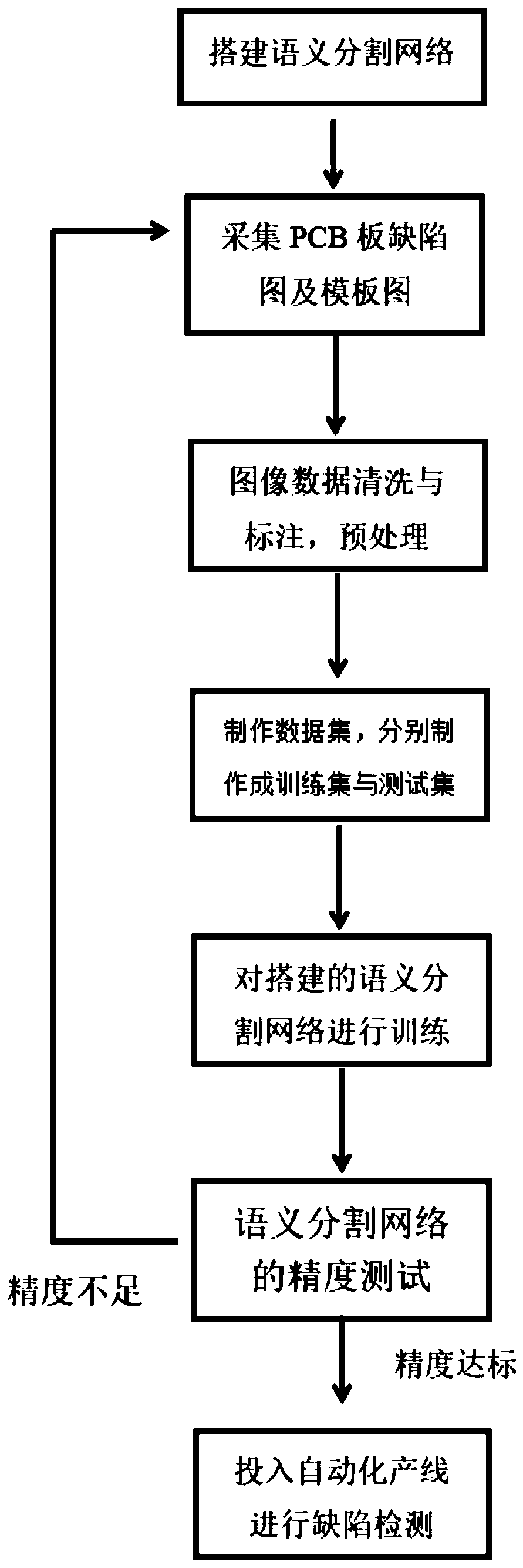
[0053] Such as figure 1 , figure 2 with image 3 As shown, the present embodiment discloses a method for detecting defects of PCB boards based on semantic segmentation, and the method for detecting defects mainly includes the following specific steps:

[0054] Step S1: Data collection and defect definition.

[0055] Specifically, the step S1 specifically includes: collecting from the factory production site a large number of PCB board pictures whose defects cannot be judged under the detection device under the traditional automated process flow and a corresponding number of template diagrams, defining the template diagram as its PCB board to be detected defects standard.

[0056] Specifically, the step S1 further includes: determining the defect type of the PCB board in combination with the requirements of the manufacturer and the knowledge of industry experts, and using semantic segmentation and marking software as an image defect marking tool for data labeling.

[0057]...

Embodiment 2

[0095] to combine Figure 1 to Figure 3 As shown, the present embodiment discloses a method for detecting defects of PCB boards based on semantic segmentation, which is characterized in that it specifically includes the following implementation steps:

[0096] Step 1: Image data acquisition and defect type definition.

[0097] Step 1.1: Collect a large number of PCB board images, unify the collected images into a size of 572*572 (length*width), and prepare the corresponding template image for each image;

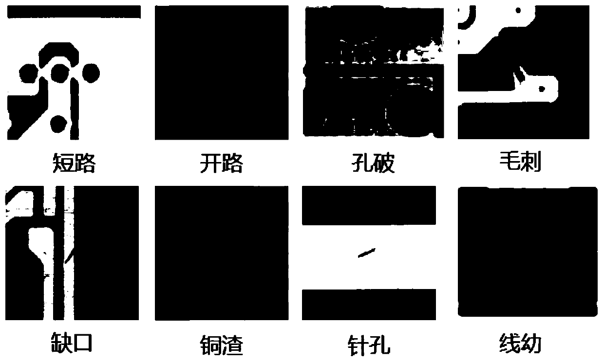
[0098] Step 1.2: Define PCB board defect type standards based on manufacturer's needs and industry knowledge. The defect types include: open circuit, short circuit, hole slope, burr, gap, copper slag, thin line, and pinhole.

[0099] Step 2: Image data cleaning and labeling.

[0100] Step 2.1: Clean the image data collected in step 1, use semantic segmentation and labeling software to mark defect features, and generate a json file for storage after marking;

[0101] Step ...


PUM


Abstract

The invention discloses a PCB defect detection method based on semantic segmentation. The PCB defect detection method comprises the following steps of S1, data collection and defect definition; S2, data annotation and cleaning are carried out; S3, image preprocessing and data set making; S4, constructing a neural network model and carrying out data training; S5, testing the model; S6, defect judgment. According to the PCB defect detection algorithm based on the built semantic segmentation network provided by the invention, PCB picture data acquired from a production field can be preprocessed and then directly sent to the model for judgment without manual intervention; compared with traditional manual screening and subsequent defect detection methods based on machine vision, after the artificial intelligence algorithm is added, a large amount of manpower is reduced, the defect detection rate and precision are greatly improved, and the performance is more excellent.

Description

technical field [0001] The invention relates to the field of PCB board defect detection, in particular to a method for detecting PCB board defects based on semantic segmentation. Background technique [0002] For a long time, the quality problems of PCB board products caused by bumps and stains in the production process have attracted the attention of manufacturers. PCB defect detection is extremely important. With the continuous expansion of PCB market demand, its defect detection task has also changed. become more difficult. [0003] In the past, the traditional PCB board defect detection method has developed from manual screening to the automatic detection stage in the industrial field, such as through machine vision and traditional image processing technology, but these methods need to consume a lot of manpower, manual misjudgment, automatic detection equipment Missed judgment, low detection efficiency and other problems. [0004] Therefore, the prior art needs to be f...

Claims


Application Information

Patent Timeline
IPC IPC(8): G06T7/00G06K9/46G06K9/62G06N3/04G01N21/88G01N21/956
CPCG06T7/0004G01N21/8851G01N21/956G06T2207/20081G06T2207/20084G06T2207/30141G01N2021/8854G01N2021/8887G01N2021/8883G01N2021/95638G06V10/40G06N3/045G06F18/241
Inventor 罗哲黄坤山
Owner FOSHAN NANHAI GUANGDONG TECH UNIV CNC EQUIP COOP INNOVATION INST
Why Eureka
Try Eureka