
Transfer device of semiconductor wafer

A transfer device, semiconductor technology, applied in semiconductor/solid-state device manufacturing, transportation and packaging, electrical components, etc., can solve problems such as looseness, complicated movements, and easy damage of three thimbles

Pending Publication Date: 2020-04-10
江苏晋誉达半导体股份有限公司
View PDF2 Cites 1 Cited by
  • Summary
  • Abstract
  • Description
  • Claims
  • Application Information

AI Technical Summary

Problems solved by technology

[0005] However, this transfer device has the following problems: firstly, the support ring only supports the wafer, but is not fixed, so it may become loose during the transfer process; secondly, this transfer fixture needs a matching lifting device and three thimbles, and at the same time It also needs a jacking action, which makes the action more complicated. At the same time, the three thimbles are easy to damage, and it is very troublesome to repair.

Method used


Image

  • Transfer device of semiconductor wafer
  • Transfer device of semiconductor wafer
  • Transfer device of semiconductor wafer

Examples


Embodiment Construction

[0028] The present invention will be described in further detail below through specific examples.

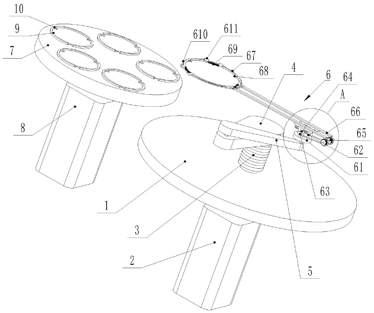
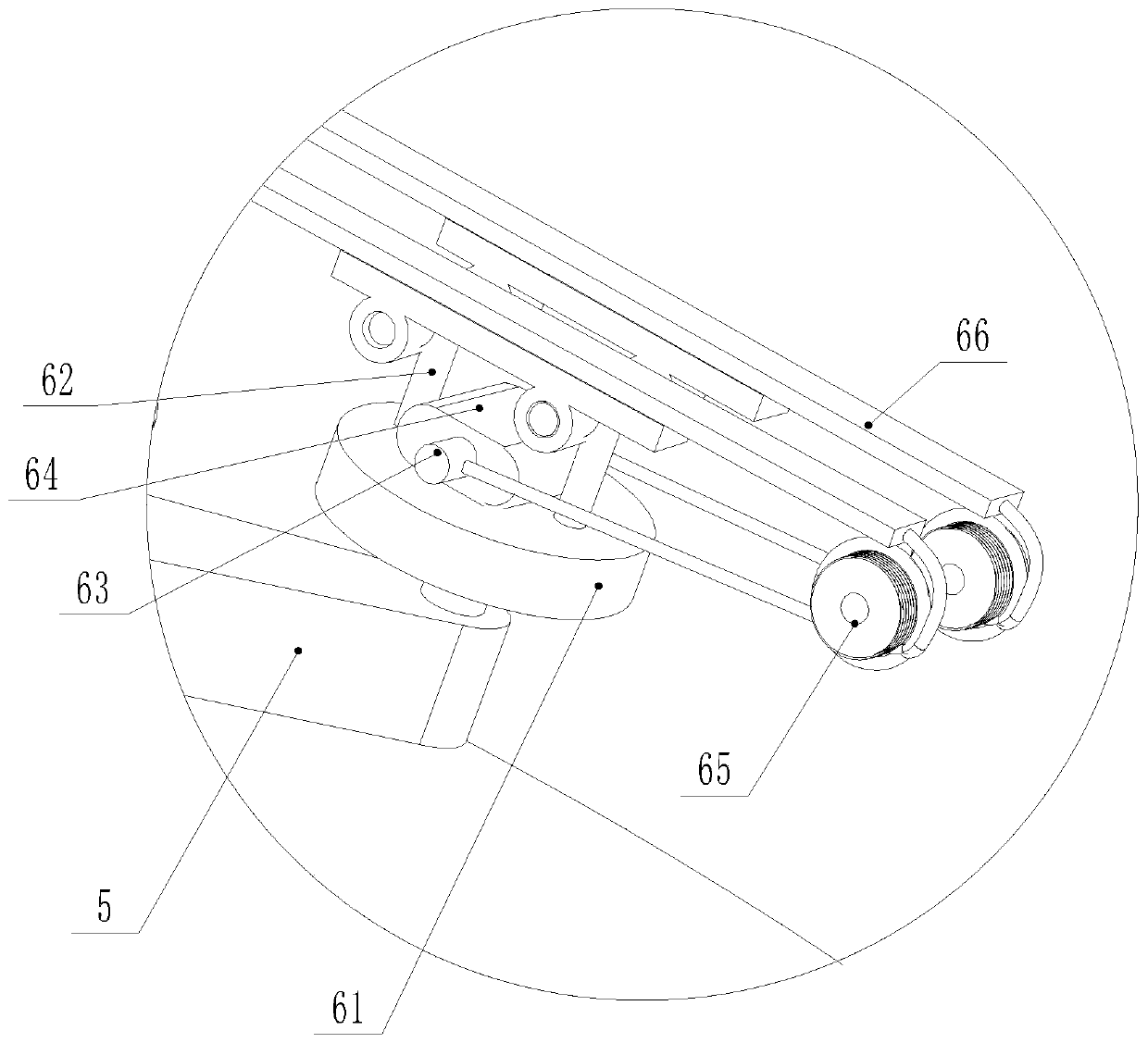
[0029] Such as Figure 1 to Figure 4 As shown, a transfer device for a semiconductor wafer includes a base 1, a transfer manipulator is installed on the base 1, a transfer gripper 6 is installed on the execution end of the transfer manipulator, and the transfer gripper 6 is controlled by the transfer manipulator when taking the sheet. Swing and lift between the station and the placement station.

[0030] Wherein, the transfer device of this embodiment can operate in a normal environment, and can also operate in a vacuum environment. For example, it operates in a vacuum environment during the etching process of a semiconductor wafer.

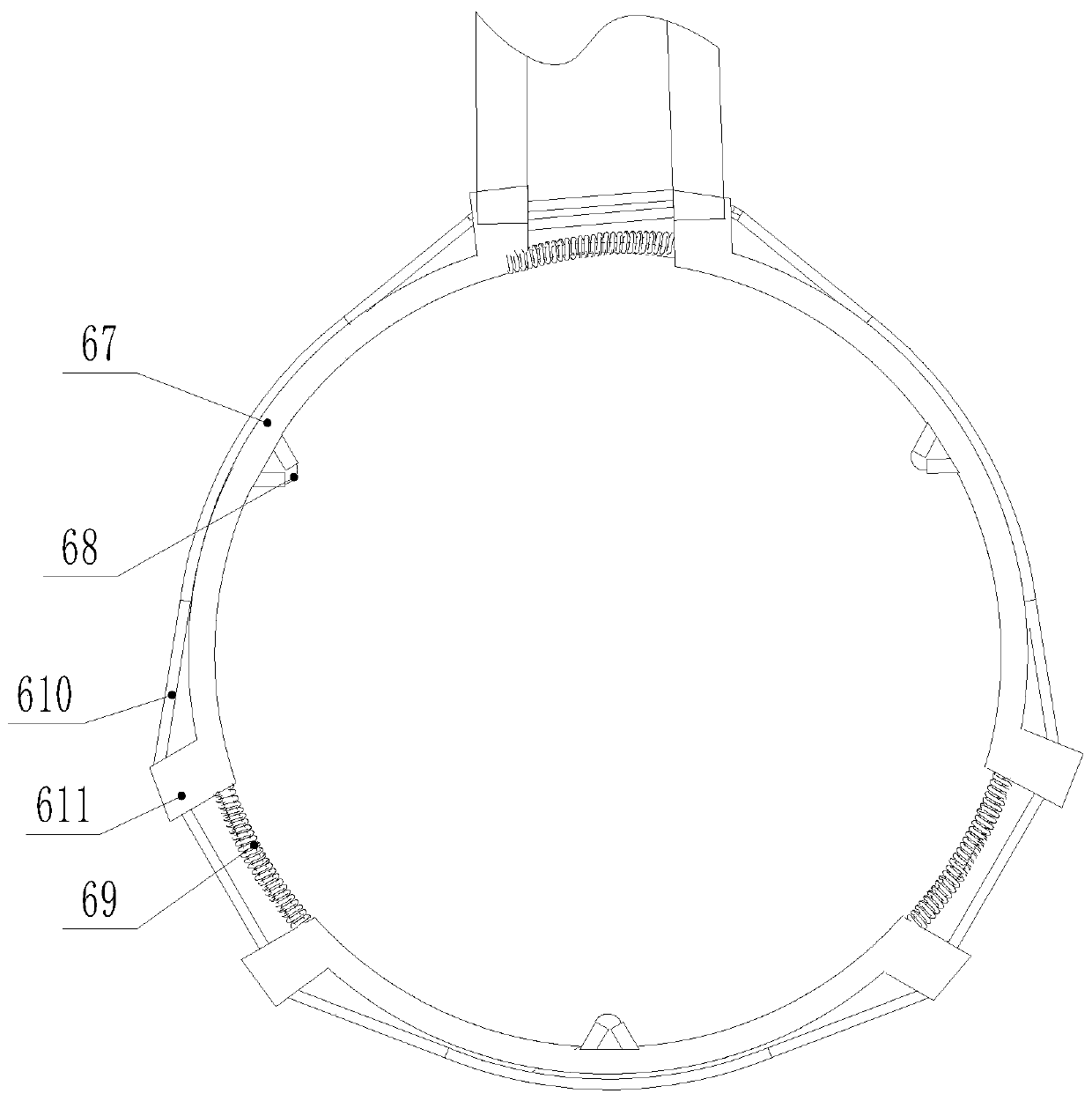
[0031]The transfer fixture 6 includes a support arm 66 and an annular clamp ring mounted on the support arm 66 for clamping the wafer, the support arm 66 is mounted on the end of the transfer manipulator, and the clamp ring includes several segme...


PUM

PropertyMeasurementUnit
angleaaaaaaaaaa

Abstract

The invention discloses a transfer device of a semiconductor wafer. The device comprises a base, a transfer manipulator and a transfer clamp, the transfer clamp comprises a supporting arm and an annular clamping ring which is installed on the supporting arm and used for clamping a wafer. The supporting arm is mounted at the tail end of the transfer manipulator; the clamping ring comprises a plurality of clamping ring sections; an arc-shaped inserting rod is arranged at one end of each clamping ring section; inserting holes matched with the arc-shaped inserting rods are formed in the other endsof the arc-shaped inserting rods; a clamping tongue is arranged at the bottom of the inner side of each clamping ring section; the bottoms of the clamping tongues are flush with the bottoms of the clamping ring sections, two adjacent clamping ring sections are installed on the supporting arm, opening and closing mechanisms for driving the clamping ring sections to be opened and closed are installed on the supporting arm and the clamping ring sections, a wafer carrying disc is arranged on a wafer taking station, a process cavity is formed in the wafer carrying disc, and notches matched with the clamping tongues in a one-to-one correspondence mode are formed in the cavity wall of the process cavity. The transfer device can well clamp the wafer, the wafer is prevented from loosening in the transferring process, jacking of an ejector pin is not needed any more, and reliability is higher.

Description

technical field [0001] The invention relates to a transfer device used for transferring semiconductor wafers. Background technique [0002] With the rapid development of my country's economic construction, the market demand for wafers is increasing, which drives the rapid development of the semiconductor wafer processing industry. [0003] In the technical field of semiconductors, a semiconductor wafer is generally a silicon wafer or a wafer of other semiconductors. At present, a wafer tray is placed on the processing station, and the wafer tray is provided with a process chamber for supporting the processed wafer. The lower part of the wafer tray is provided with a lifting device, and the lifting device is inserted with a thimble. When processing wafers, the wafers are generally sent into or removed from the process chamber by a special transfer device. [0004] However, the current transfer device includes a base on which a transfer manipulator is installed. A transfer ...

Claims


Application Information

Patent Timeline
Patent Type & Authority Applications(China)
IPC IPC(8): H01L21/677H01L21/687
CPCH01L21/67742H01L21/68707
Inventor 丁桃宝丁烨滨周琛怿
Owner 江苏晋誉达半导体股份有限公司
Learn More