A Design Method to Solve the Production Deviation of qfn Package Parts
A design method and packaging-like technology, applied in the server field, to increase the welding area, improve the welding quality, and ensure the welding reliability.
- Summary
- Abstract
- Description
- Claims
- Application Information
AI Technical Summary
Problems solved by technology
Method used
Image
Examples
Embodiment Construction
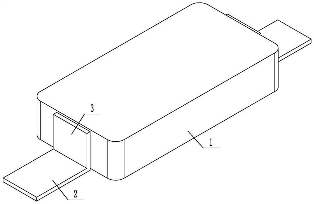
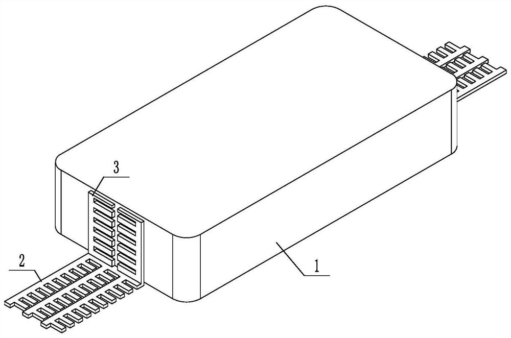
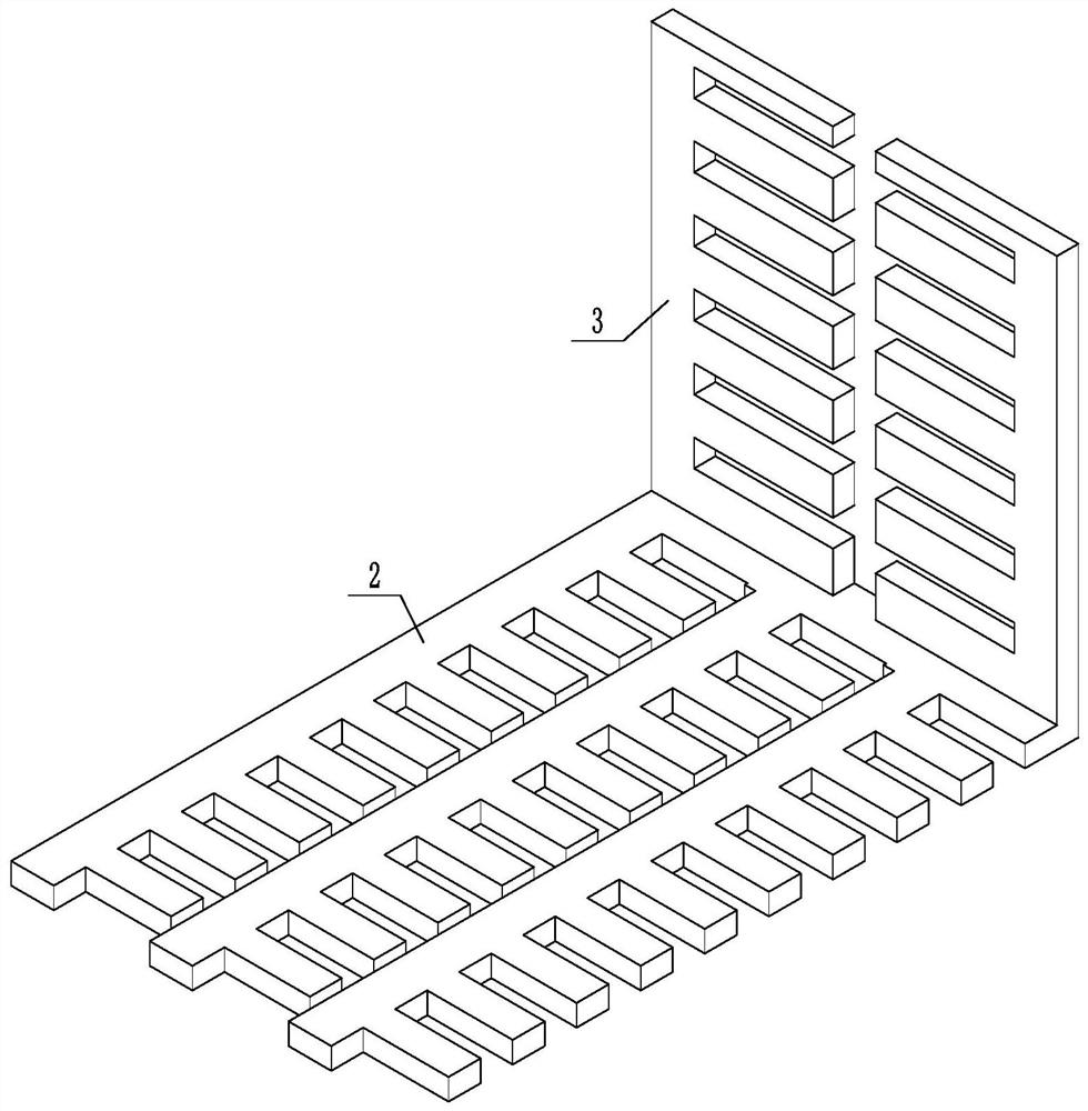
[0018] Such as Figure 1 to 3 As shown, a design method for solving the production of partial production of the QFN package, its steps are:
[0019] 1) The bottom surface of the package part extends to both sides to form an epitaxial horizontal pin and a vertical lead in the vertical direction. See figure 1 As shown in the present embodiment, the package part is a crystal oscillator 1, and the crystal bottom surface pin extends to the outside of the crystal bottom surface to form an epitaxial horizontal pin 2, and a vertical lead 3 is provided on the epitaxial pin 3. Due to the increase of the epitaxial level pin, it is equivalent to increasing the entire area of the bottom surface pin of the crystal, which is more stable when the entire crystal hit is placed on the PCB, and the welding is not easily offset; the design of the vertical pin makes the side surface also solder The part can increase the welding area of the entire part.
[0020] 2) Inside the epitaxial horizontal pin...
PUM
 Abstract
Description
Claims
Application Information


