Organic compounds and electronic devices
A technology of organic compounds and electronic devices, applied in organic chemistry, chemical instruments and methods, circuits, etc., can solve problems such as performance degradation of light-emitting devices, increase of driving voltage, and reduction of luminous efficiency, so as to improve life characteristics, inhibit material crystallization, Enhanced Injection and Delivery Effects
- Summary
- Abstract
- Description
- Claims
- Application Information
AI Technical Summary
Problems solved by technology
Method used
Image

Examples
preparation example Construction
[0062] The preparation method of the compound of the embodiment of the present invention is described in detail below:
[0063] Synthesis of compound 1
[0064]
[0065] Magnesium bars (15.44 g, 643.5 mmol) and diethyl ether (100 mL) were placed in a dry round bottom flask under nitrogen, and iodine (119 mg) was added. Then a solution of ether (200mL) dissolved with 2-bromobiphenyl 2-bromotoluene (50.00g, 214.49mmol) was slowly dropped into the flask, and after the addition was completed, the temperature was raised to 35°C and stirred for 3 hours; the reaction solution was lowered to 0°C, a solution of ether (200mL) dissolved with adamantanone (48.33g, 321.7mmol) was slowly dropped into it, and after the addition was completed, the temperature was raised to 35°C and stirred for 6 hours; the reaction solution was cooled to room temperature, and added 5% hydrochloric acid to pH<7, stirred for 1 hour, added diethyl ether (200mL) for extraction, combined the organic phases, dr...
Embodiment 1
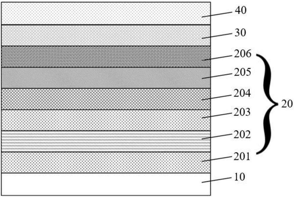
[0183] The anode 10 is prepared by the following process: the thickness is The ITO substrate was cut into a size of 40mm × 40mm × 0.7mm, and it was prepared into a top emission experimental substrate with a cathode overlapping area, an anode and an insulating layer pattern by using a photolithography process, using ultraviolet ozone and O 2 :N 2 Plasma is used for surface treatment to increase the work function of the anode (experimental substrate) and to clean the experimental substrate.
[0184] On the experimental substrate (anode 10) vacuum evaporation HAT-CN to form a thickness of The hole injection layer (HIL) 201.
[0185] NPB is vacuum evaporated on the hole injection layer 201 to form a thickness of The hole transport layer (HTL) 202.
[0186] Evaporate TCTA on the hole transport layer 202 to form a thickness of Electron blocking layer (EBL) 203 .
[0187] α, β-ADN is used as the main body, and BD-1 is doped with a doping ratio of 3%, and evaporated on the e...
Embodiment 2-19
[0197] The organic electroluminescence device was fabricated by the same method as in Example 1, except that the compounds shown in Table 1 were used instead of Compound 1 when forming the electron transport layer (ETL) 206 .
PUM
| Property | Measurement | Unit |
|---|---|---|
| electron mobility | aaaaa | aaaaa |
Abstract
Description
Claims
Application Information
 - R&D Engineer
- R&D Manager
- IP Professional
- Industry Leading Data Capabilities
- Powerful AI technology
- Patent DNA Extraction
Browse by: Latest US Patents, China's latest patents, Technical Efficacy Thesaurus, Application Domain, Technology Topic.
© 2024 PatSnap. All rights reserved.Legal|Privacy policy|Modern Slavery Act Transparency Statement|Sitemap